 | –≠–ª–µ–∫—Ç—Ä–æ–Ω–Ω—ã–π –∫–æ–º–ø–æ–Ω–µ–Ω—Ç: MP7636 | –°–∫–∞—á–∞—Ç—å:  PDF PDF  ZIP ZIP |
MP7636A
1
Rev. 2.00
FEATURES
∑
Four Quadrant Multiplication
∑
16-Bit Monotonicity
∑
Lower Data Bus Feedthrough @ CS = 1
∑
Low Feedthrough Error
∑
Low Power Consumption
∑
TTL/5 V CMOS Compatible
∑
Double Buffered
∑
Decoded DAC Approach
∑
Latch-Up Free
15 V CMOS Microprocessor Compatible
Double-Buffered, Multiplying 16-Bit
Digital-to-Analog Converter
BENEFITS
∑
High Accuracy Performance at Low Cost
∑
Easy Interface with 8-Bit Microprocessors
∑
Simple Upgrade of MP1230A Family to High
Accuracy (Pin Compatible)
∑
Reduced Board Space
∑
16-Bit Bus Version: MP7626
GENERAL DESCRIPTION
The MP7636A is manufactured using advanced thin film
resistors on a double metal CMOS process. The MP7636A
incorporates a unique bit decoding technique yielding lower
glitch, higher speed and excellent accuracy over temperature
and time. 16-bit differential non-linearity is achieved with
minimal laser trim.
The MP7636A is packaged in a 20-pin 300 mil wide DIP and is
a direct 16-bit replacement for the 12-bit DAC1230 series. Full
pin-for-pin compatibility allows existing systems to be upgraded
to 16 bits without hardware modification.
The MP7636A provides 16-bit data loading through 8 input
data lines for direct interface to 8-bit data buses. All data loading
and data transfer operations are identical to the WRITE cycle of
a static RAM.
The MP7636A uses a unique circuit which significantly
reduces transients in the supplies during DATA bus transitions
at CS = 1.
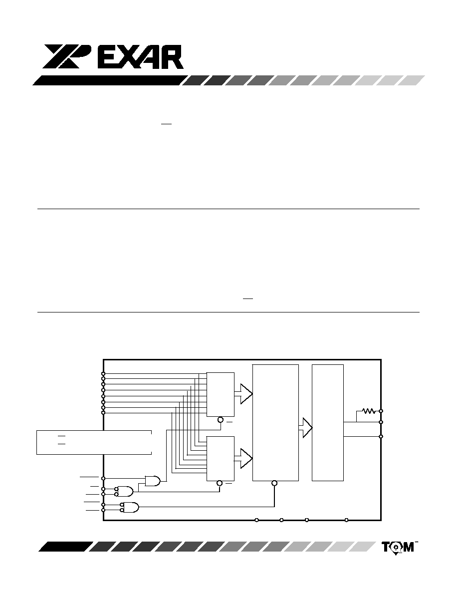
SIMPLIFIED BLOCK DIAGRAM
DGND
AGND
DB15 (MSB)
(DB7)
DB14
(DB6)
DB13
(DB5)
DB12
(DB4)
DB11
(DB3)
DB10
(DB2)
DB9
(DB1)
DB8 (DB0, LSB)
BYTE1/BYTE2
CS
WR1
XFER
WR2
8-Bit
Input
Latch
16-Bit
Register
16-Bit
MDAC
LE
LE
When LE = 1 latch outputs follow inputs
When LE = 0 Latch outputs are latched
R
FB
I
OUT1
I
OUT2
V
DD
V
REF
8-Bit
Input
Latch
MP7636A
2
Rev. 2.00
ORDERING INFORMATION
Package
Type
Temperature
Range
Part No.
SOIC
SOIC
≠40 to +85
∞
C
+2
+2
MP7636AJS
+4
+4
MP7636AKS
0.1
≠40 to +85
∞
C
0.1
INL
(LSB)
Gain Error
(% FSR)
DNL
(LSB)
*Contact factory for non-compliant military processing
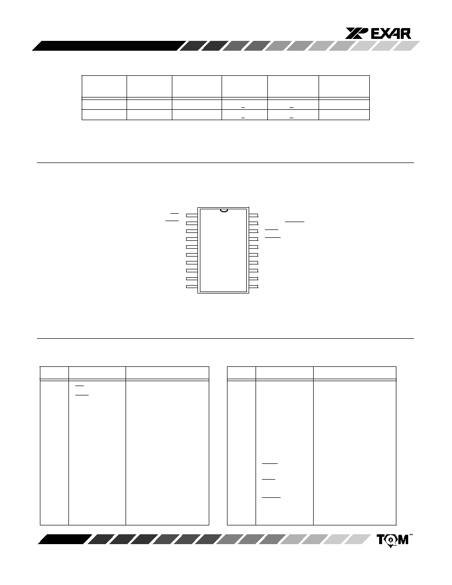
PIN CONFIGURATION
20
1
11
10
2
3
4
5
6
7
15
14
13
12
17
16
8
9
19
18
DB12 (DB4)
DB13 (DB5)
DB14 (DB6)
DB15 (MSB) (DB7)
V
DD
I
OUT2
I
OUT1
AGND
DB11 (DB3)
DB10 (DB2)
DB9 (DB1)
DB8 (DB0, LSB)
DGND
R
FB
V
REF
20 Pin SOIC (Jedec, 0. 300")
S20
See Packaging Section for Package Dimensions
CS
WR1
BYTE1/BYTE2
WR2
XFER
PIN OUT DEFINITIONS
PIN NO.
NAME
DESCRIPTION
1
CS
Chip Select (Active Low)
2
WR1
Write1 (Active Low)
3
AGND
Analog Ground
4
DB11
Data Input Bit 11 (MSB)
(DB3)
Data Input Bit 3
5
DB10
Data Input Bit 10
(DB2)
Data Input Bit 2
6
DB9
Data Input Bit 9
(DB1)
Data Input Bit 1
7
DB8
Data Input Bit 8
(DB0)
Data Input Bit 0 (LSB)
8
V
REF
Reference Input Voltage
9
R
FB
Internal Feedback
Resistor
10
DGND
Digital Ground
11
I
OUT1
Current Output 1
12
I
OUT2
Current Output 2
13
DB15 (MSB)
Data Input Bit 15
(DB7)
(Most Significant Bit)
Data Input Bit 7
14
DB14
Data Input Bit 14
(DB6)
Data Input Bit 6
15
DB13
Data Input Bit 13
(DB5)
Data Input Bit 5
16
DB12
Data Input Bit 12
(DB4)
Data Input Bit 4
17
XFER
Transfer Control Signal
(Active Low)
18
WR2
Write 2 (Active Low)
19
BYTE1/
Byte Sequence Control
BYTE2
20
V
DD
Power Supply
PIN NO.
NAME
DESCRIPTION
MP7636A
3
Rev. 2.00
ELECTRICAL CHARACTERISTICS
(V
DD
= + 15 V, V
REF
= +10 V unless otherwise noted)
25
∞
C
Tmin to Tmax
Parameter
Symbol
Min
Typ
Max
Min
Max
Units
Test Conditions/Comments
STATIC PERFORMANCE
1
FSR = Full Scale Range
Resolution (All Grades)
N
16
16
Bits
Integral Non-Linearity
INL
LSB
Best Fit Straight Line Spec.
(Relative Accuracy)
(Max INL ≠ Min INL) / 2
J, S
+4
+4
K, L, T
+2
+2
Differential Non-Linearity
DNL
LSB
All grades guaranteed
J, S
+4
+4
monotonic over full
K, T
+2
+2
operating temperature
L
+1
+2
range.
Gain Error
GE
+0.1
+0.1
% FSR
Using Internal R
FB
Gain Temperature Coefficient
2
TC
GE
+2
ppm/
∞
C
Gain/
Temperature
Power Supply Rejection Ratio
PSRR
+50
+50
ppm/%
|
Gain/
V
DD
|
V
DD
= + 5%
Output Leakage Current
I
OUT
+10
+200
nA
I
OUT1
only
DYNAMIC PERFORMANCE
2
Current Settling Time
t
S
2
µ
s
To 1/2 LSB
R
L
=100
, C
EXT
=13pF
AC Feedthrough at I
OUT1
F
T
2
mV p-p
V
REF
= 20 V p-p
Sine wave @ 10kHz
REFERENCE INPUT
Input Resistance
R
IN
2.5
7.5
2.5
7.5
k
LOGIC INPUTS
3
Input High Voltage
V
INH
3.0
2.4
3.0
V
Input Low Voltage
V
INL
0.8
0.8
V
Input Current
I
LKG
+1
+1
µ
A
Input Capacitance
Data C
IN
5
pF
Control
C
IN
5
pF
ANALOG OUTPUTS
2
Output Capacitance
C
OUT1
280
pF
DAC all 1's
C
OUT1
120
pF
DAC all 0's
C
OUT2
100
pF
DAC all 1's
C
OUT2
240
pF
DAC all 0's
MP7636A
4
Rev. 2.00
ELECTRICAL CHARACTERISTICS (CONT'D)
Parameter
Symbol
Min
Typ
Max
Min
Max
Units
Test Conditions/Comments
POWER SUPPLY
5
Functional Voltage Range
2
V
DD
4.5
16.5
5.0
16.5
V
Supply Current
I
DD
1
1
mA
All digital inputs 0 V or V
DD
SWITCHING
CHARACTERISTICS
2, 4
CS to WR Set-Up Time
t
CS
150
ns
CS to WR Hold Time
t
CH
10
ns
Data Valid to WR Set-Up Time
t
DS
70
ns
Data Valid to WR Hold Time
t
DH
70
ns
WR, XFER Pulse Width
t
W
150
ns
NOTES:
Specifications are subject to change without notice
25
∞
C
Tmin to Tmax
(1)
Full Scale Range (FSR) is 10V for unipolar mode.
(2)
Guaranteed but not production tested.
(3)
Digital input levels should not go below ground or exceed the positive supply voltage, otherwise damage may occur.
(4)
See timing diagram.
(5)
Specified values guarantee functionality. Refer to other parameters for accuracy.
ABSOLUTE MAXIMUM RATINGS (T
A
= +25
∞
C unless otherwise noted)
1, 2, 3
Voltage at Any Digital Input
GND ≠0.5 to V
DD
+0.5 V
. . . . .
Voltage at V
REF
Input
+25 V
. . . . . . . . . . . . . . . . . . . . . . . . . . .
DC Voltage Applied to I
OUT1
or I
OUT2
GND ≠0.5 V to +17 V
Supply Voltage (V
DD
)
+17 V
DC
. . . . . . . . . . . . . . . . . . . . . . . .
AGND to DGND
+1 V
. . . . . . . . . . . . . . . . . . . . . . . . . . . . . . . . .
(Functionality Guaranteed +0.5 V)
Storage Temperature Range
≠65
∞
C to 150
∞
C
. . . . . . . . . . . .
Package Power Dissipation Rating to 75
∞
C
SOIC
900mW
. . . . . . . . . . . . . . . . . . . . . . . . . . . . . . . . . . . . . . .
Derates above 75
∞
C
12mW/
∞
C
. . . . . . . . . . . . . . . . . . . . . . . .
NOTES:
1
Stresses above those listed under "Absolute Maximum Ratings" may cause permanent damage to the device. This is a
stress rating only and functional operation at or above this specification is not implied. Exposure to maximum rating
conditions for extended periods may affect device reliability.
2
Any input pin which can see a value outside the absolute maximum ratings
should be protected by Schottky diode clamps
(HP5082-2835) from input pin to the supplies.
All inputs have protection diodes which will protect the device from short
transients outside the supplies of less than 100mA for less than 100
µ
s.
3
GND refers to AGND and DGND.
APPLICATION NOTES
Refer to Section 8 for Applications Information
MP7636A
5
Rev. 2.00
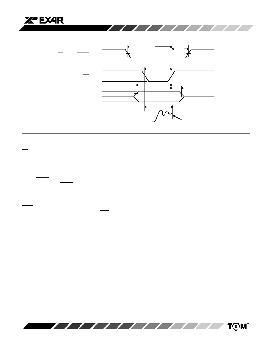
TIMING DIAGRAM
50%
50%
50%
50%
50%
50%
SETTLED TO
+0.01%
CS, BYTE1/BYTE2
WR
DATA BITS
V
IH
V
IL
V
IH
V
IL
V
IH
V
IL
t
CS
t
CH
t
W
t
DS
t
S
t
DH
I
OUT1,
I
OUT2
DEFINITION OF CONTROL SIGNALS:
CS:
Chip Select (Active low).
It will enable WR1.
WR1:
Write 1 (Active low)
The WR1 is used to load the digital data bits (DB) into
the input latch.
BYTE1/BYTE2:
Byte sequence control.
The BYTE1/BYTE2 control pin is used to select MSB
and LSB both input latches.
WR2:
Write 2 (Active low).
It will enable XFER.
XFER:
Transfer control signal (Active low).
This signal, in combination with WR2, causes the
16-bit data which is available in the input latches to
transfer to the DAC register.
DB0 to DB15: Digital Inputs.
DB0 is the least significant digital input (LSB) and
DB15 is the most significant digital input (MSB).
I
OUT1
:
DAC Current Output 1 Bus.
I
OUT1
is a maximum for a digital code of all 1's in the
DAC register, and is zero for all 0's in the DAC register.
I
OUT2
:
DAC Current Output 2 Bus.
I
OUT2
is a complement of I
OUT1
. The ladder termina-
tion has been tied to I
OUT2
internally.
R
FB
:
Feedback Resistor.
This internal feedback resistor should always be used
(not an external resistor) since it matches the resistors
in the DAC and tracks these resistor over temperature.
V
REF
:
Reference Voltage Input.
This input connects an external precision voltage
source to the internal DAC. The V
REF
can be selected
over the range of +25V to ≠25V or the analog signal for
a 4-quadrant multiplying mode application.
V
DD
:
Power Supply Voltage.
This is the power supply pin for the part. The V
DD
can
be from +5 V DC to +15 V
DC, however optimum volt-
age is +15 V DC.
AGND: Analog Ground.
Back gate of the DAC N-channel current steering
switches.
DGND: Digital Ground .
The timing diagrams for updating the DAC register are shown
in
Figures 1 and 2.