 | –≠–ª–µ–∫—Ç—Ä–æ–Ω–Ω—ã–π –∫–æ–º–ø–æ–Ω–µ–Ω—Ç: MP7641AS | –°–∫–∞—á–∞—Ç—å:  PDF PDF  ZIP ZIP |

MP7641
1
Rev. 2.00
8-Channel Voltage Output
10 MHz Input Bandwidth 8-Bit
Multiplying DACs with
Serial Digital Port
FEATURES
∑
8 Independent 2-Quadrant Multiplying 8-Bit DACs
∑
Dual Positive (+10 V and +5 V) Supplies or
Dual (+5 V) Supplies Capability
∑
High Speed:
≠
12.5 MHz Digital Clock Rate
≠
V
REF to
V
OUT
Settling Time: 150ns to 8≠bit
(typ)
≠
Voltage Reference Input Bandwidth:
10 MHz
∑
Low Power: 150mW
∑
Low AC Voltage Reference Feedthrough
∑
Excellent Channel-to-Channel Isolation
∑
DNL = +0.8 LSB, INL = +1 LSB (typ)
∑
DACs Matched to +0.5% (typ)
∑
Chip Select Available: MP7651
∑
Low Harmonic Distortion: 0.25% typical with
V
REF
= 1 V p-p @ 1 MHz
∑
V
REF
/2 Output Preset Level
∑
Latch-Up Free
∑
ESD Protection: 2000 V Minimum
APPLICATIONS
∑
Direct High-Frequency Automatic Gain Control
∑
Video AGC & CCD Level AGC
∑
Convergence Adjustment for High-Resolution
Monitors (Workstations)
GENERAL DESCRIPTION
The MP7641 is ideal for direct gain control of video, compos-
ite video, CCD and other high frequency analog signals. The de-
vice includes 8-channels of high speed, high bandwidth, two
quadrant multiplying, 8-bit accurate digital-to-analog converter.
It includes an output drive buffer per channel capable of driving a
+1mA (typ) to a load. DNL of better than +0.8 LSB is achieved
with a channel-to-channel matching of better than 0.5% (typ).
Stability, matching, and precision of the DACs are achieved by
using EXAR's thin film technology. Also, excellent channel-to-
channel isolation is achieved with EXAR's BiCMOS process
which cannot be achieved using a typical CMOS technology.
An open loop architecture (patent pending) provides wide
small signal bandwidth from V
REF
to output up to 10 MHz (typ),
fast output settling time, and V
REF
feedthrough isolation of
≠65dB or better. In addition, low distortion in the order of 0.25%
with a 1 V p-p, 1 MHz signal is achieved.
The combination of a constant input Z and the ability to vary
AGND within +300 mV allows flexibility for optimum system de-
sign.
The MP7641 has a serial data 3-wire standard
µ
-processor
logic interface to reduce pin count, package size, and board wire
(space).
The MP7641 is fabricated on a junction isolated, high speed
BiCMOS (BiCMOS IV
TM
) process with thin film resistors. This
process enables precision high speed analog/digital (mixed-
mode) circuits to be fabricated on the same chip.

MP7641
2
Rev. 2.00
SIMPLIFIED BLOCK DIAGRAM
©
DGND
SDO
CLK
RST
1-Bit
Latch
SDI
12-Bit Shift Register
DB0 to DB7
4-Bit Address
LD
AGND
8
V
EE
V
CC
V
DD
V
O0
V
O7
DAC 0
DAC 7
DAC 1
8-Bit Latch
8-Bit Latch
8-Bit Latch
4-8 DEC
8
8
8
8
3-State
Buffer
V
O1
8
4
LD
+1
+1
+1
1-Bit
Latch
V
R0
V
R1
V
R7
ORDERING INFORMATION
Package
Type
Temperature
Range
Part No.
SOIC
≠40 to +85
∞
C
MP7641AS
+0.8
+1
+1.5
Plastic Dip
≠40 to +85
∞
C
MP7641AN
+0.8
+1
+1.5
INL
(LSB)
Gain Error
(% FSR)
DNL
(LSB)

MP7641
3
Rev. 2.00
PIN CONFIGURATIONS
13
16
14
15
1
2
3
4
5
6
7
8
9
10
28
27
26
25
24
23
22
21
20
19
11
18
12
17
28 Pin PDIP (0.300")
NN28
AGND
DGND
AGND
CLK
SDI
AGND
V
DD
V
CC
V
EE
SDO
28 Pin SOIC (EIAJ, 0.335")
R28
28
1
15
14
2
3
4
5
6
7
17
16
8
9
19
18
10
11
23
22
21
20
27
26
25
24
12
13
V
O1
V
O2
V
R2
V
R3
V
O3
V
O4
V
R4
V
R5
V
O5
V
R1
V
R0
V
O0
V
O7
V
R7
V
R6
V
O6
AGND
CLK
SDI
AGND
SDO
V
R1
V
R0
V
O0
V
O7
V
R7
V
R6
V
O6
AGND
DGND
V
DD
V
CC
V
EE
V
O1
V
O2
V
R2
V
R3
V
O3
V
O4
V
R4
V
R5
V
O5
RST
LD
RST
LD
See Packaging Section for Package Dimensions
PIN OUT DEFINITIONS
1
V
O1
DAC 1 Output
2
V
O2
DAC 2 Output
3
V
R2
DAC 2 Reference Input
4
V
R3
DAC 3 Reference Input
5
V
O3
DAC 3 Output
6
V
DD
Digital Positive Supply
7
V
CC
Analog Positive Supply
8
V
EE
Analog Negative Supply
9
AGND
Analog Ground
10
DGND
Digital Ground
11
V
O4
DAC 4 Output
12
V
R4
DAC 4 Reference Input
13
V
R5
DAC 5 Reference Input
14
V
O5
DAC 5 Output
15
V
O6
DAC 6 Output
PIN NO.
NAME
DESCRIPTION
16
V
R6
DAC 6 Reference Input
17
V
R7
DAC 7 Reference Input
18
V
O7
DAC 7 Output
19
AGND
Analog Ground
20
SDI
Serial Data/Address Input
21
SDO
Serial Data Output
22
CLK
Shift Register Clock
23
LD
Load Signal; Load Data
to Selected DACs
24
RST
Reset Signal; Reset all DACs to
V
REF
/2
25
AGND
Analog Ground
26
V
O0
DAC 0 Output
27
V
R0
DAC 0 Reference Input
28
V
R1
DAC 1 Reference Input
PIN NO.
NAME
DESCRIPTION

MP7641
4
Rev. 2.00
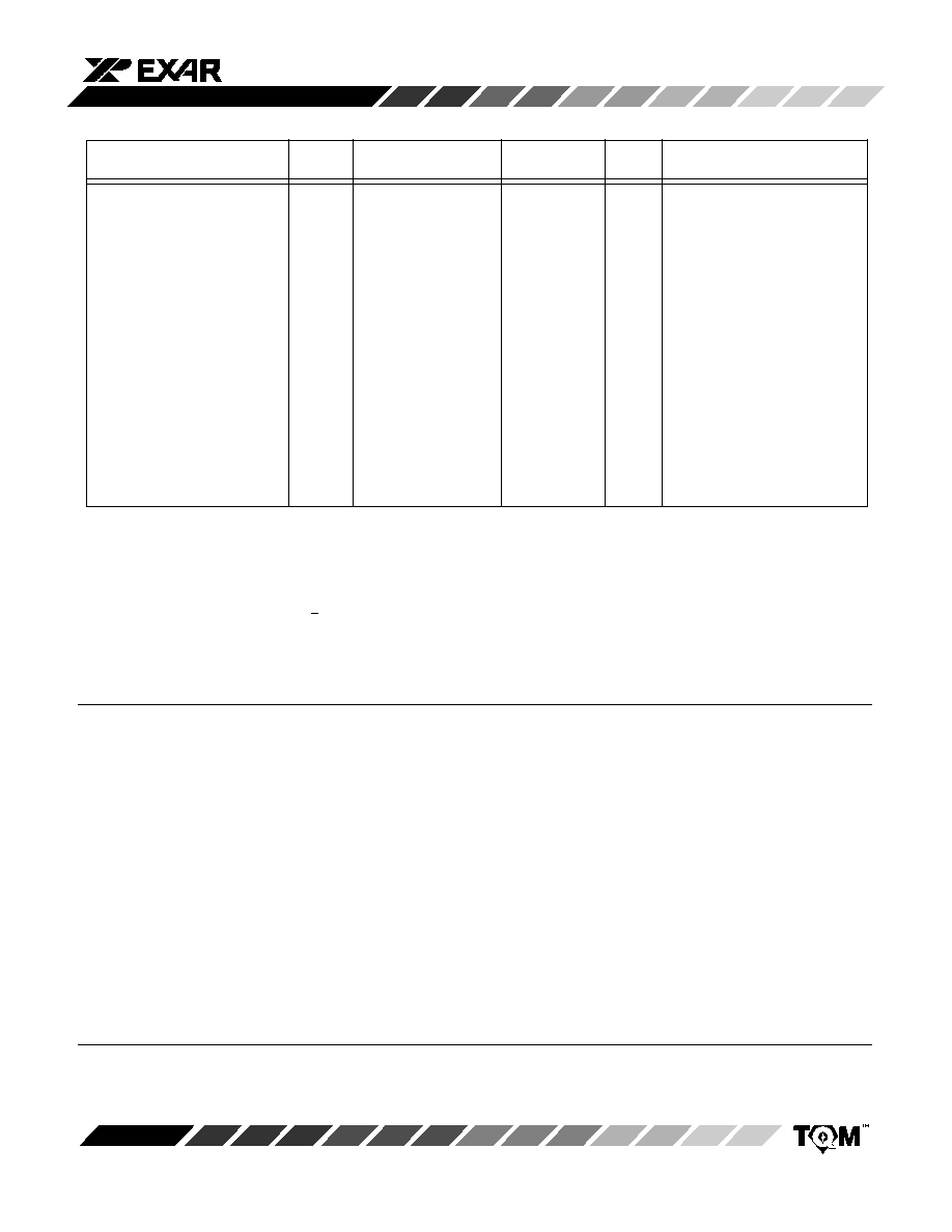
ELECTRICAL CHARACTERISTICS TABLE FOR DUAL SUPPLIES
Unless Otherwise Noted: V
DD
= 5 V, V
CC
= +5 V, V
EE
= ≠5 V, V
REF
= 3 V and ≠3 V, T = 25
∞
C,
Output Load = Open, AGND=DGND=0 V
25
∞
C
Tmin to Tmax
Parameter
Symbol
Min
Typ
Max
Min
Max
Units
Test Conditions/Comments
DC CHARACTERISTICS
Resolution (All Grades)
N
8
8
Bits
Differential Non-Linearity
DNL
+0.8
+1
LSB
Integral Non-Linearity
INL
+1
+1
LSB
Monotonicity
Guaranteed Guaranteed
Gain Error
GE
+1.5
+1.5
% FSR
FSR = Full Scale Range
1
Zero Scale Offset
Z
OFS
+20
+75
+75
mV
Output Drive Capability
I
O
+1
mA
REFERENCE INPUTS
Impedance of V
REF
REF
6
12
18
6
18
k
Voltage Range
V
R
V
EE
+1.5
V
CC
≠1.8
V
V
REF
Max Swing is AGND +3 V
DYNAMIC
CHARACTERISTICS
2
R
L
= 5 k, C
L
= 20 pF
Input to Output Bandwidth
10
MHz
V
R
= 1.6 V p≠p, R
L
= 5k
to V
EE
Input to Output Settling Time
5
150
ns
V
R
= 1.6 V p≠p, R
L
= 5k
to V
EE
Small Signal Voltage Reference
t
r
10
MHz
V
OUT
=50mV p-p above code 16
Input to Output Bandwidth
Small Signal Voltage Reference
t
r
5
8
MHz
V
OUT
=50mV p-p for all codes
Input to Output Bandwidth
Voltage Settling from V
REF
to
t
sr
275
300
325
ns
V
R
=0 to V
R
= 3V Step
6
V
DAC
Out
to 1 LSB
Voltage Settling from Digital
t
sd
275
300
325
ns
ZS to FS to 1 LSB
Code to V
DAC
Out
V
REF
Feedthrough
F
DT
≠65
dB
Codes=0 @ 1 MHz
Group Delay
GD
20
ns
Harmonic Distortion
T
HD
0.5
%
V
REF
=1MHz Sine 3V p-p
Channel-to-Channel Crosstalk
C
T
≠75
dB
@ 1 MHz, single channel
Digital Feedthrough
Q
1
nVS
CLK to V
OUT
Power Supply
PSRR
0.02
%/%
V=+5%
Rejection Ratio
POWER CONSUMPTION
Positive Supply Current
I
CC
15
25
30
mA
V
REF
= 0 V
Negative Supply Current
I
EE
15
25
30
mA
V
REF
= 0 V
Power Dissipation
P
DISS
150
250
300
mW
V
REF
= 0 V, Codes = all 1
DIGITAL INPUT
CHACTERISTICS
Logic High
3
V
IH
2.4
2.4
V
Logic Low
3
V
IL
0.8
0.8
V
Input Current
I
L
+10
+10
µ
A
Input Capacitance
2
C
L
8
8
pF

MP7641
5
Rev. 2.00
ELECTRICAL CHARACTERISTICS TABLE
Description
Symbol
Min
Typ
Max
Min
Max
Units
Conditions
DIGITAL TIMING
SPECIFICATIONS
2, 4
Input Clock Pulse Width
t
CH
, t
CL
40
50
ns
Data Setup Time
t
DS
10
10
ns
Data Hold Time
t
DH
15
15
ns
CLK to SDO Propagation Delay
t
PD
40
50
ns
DAC Register Load Pulse Width
t
LD
100
100
ns
Reset Pulse Width
t
RST
50
60
ns
Clock Edge to Load Rising Edge
t
CKLD1
100
100
ns
Clock Edge to Load Falling Edge
t
CKLD2
0
0
ns
Load Falling Edge to SDO
t
HZ1
50
60
ns
3-state Enable
Load Rising Edge to SDO
t
HZ2
35
50
ns
3-state Disable
Load Falling Edge to CLK Disable
t
LDCK1
25
40
ns
Load Rising Edge to CLK Enable
t
LDCK2
35
50
ns
LD Set-up Time with Respect
t
LDSU
15
20
ns
to CLK
25
∞
C
NOTES
1
Full Scale Range (FSR) is 3V.
2
Guaranteed but not production tested.
3
Digital input levels should not go below ground or exceed the positive supply voltage, otherwise damage may occur.
4
See Figures 2 and 3.
5
For reference input pulse: t
R
= t
F
> 100 ns.
Tmin to Tmax
Specifications are subject to change without notice

MP7641
6
Rev. 2.00
ELECTRICAL CHARACTERISTICS TABLE FOR DUAL POSITIVE SUPPLIES
Unless Otherwise Noted: V
DD
= 5 V, V
CC
= 10 V, V
EE
= 0 V, V
REF
= 3 V and ≠3 V, T = 25
∞
C,
Output Load = Open, AGND = (V
CC
+ V
EE
)/2 = 5 V, DGND = 0 V
25
∞
C
Tmin to Tmax
Parameter
Symbol
Min
Typ
Max
Min
Max
Units
Test Conditions/Comments
DC CHARACTERISTICS
Resolution (All Grades)
N
8
8
Bits
Differential Non-Linearity
DNL
+0.8
+1
LSB
Integral Non-Linearity
INL
+1
+1
LSB
Monotonicity
Guaranteed Guaranteed
Gain Error
GE
+1.5
+1.5
% FSR
FSR = Full Scale Range
1
Zero Scale Offset
Z
OFS
+20
+75
+75
mV
Output Drive Capability
I
O
+1
mA
REFERENCE INPUTS
Impedance of V
REF
REF
6
12
18
6
18
k
Voltage Range
V
R
V
EE
+1.5
V
CC
≠1.8
V
V
REF
Max Swing is AGND +3 V
DYNAMIC
CHARACTERISTICS
2
R
L
= 5 k, C
L
= 20 pF
Input to Output Bandwidth
10
MHz
V
R
= 1.6 V p≠p, R
L
= 5k
to V
EE
Input to Output Settling Time
5
150
ns
V
R
= 1.6 V p≠p, R
L
= 5k
to V
EE
Small Signal Voltage Reference
t
r
10
MHz
V
OUT
=50mV p-p above code 16
Input to Output Bandwidth
Small Signal Voltage Reference
t
r
5
8
MHz
V
OUT
=50mV p-p for all codes
Input to Output Bandwidth
Voltage Settling from V
REF
to
t
sr
275
300
325
ns
V
R
=0 to V
R
= 3V Step
6
V
DAC
Out
to 1 LSB
Voltage Settling from Digital
t
sd
275
300
325
ns
ZS to FS to 1 LSB
Code to V
DAC
Out
V
REF
Feedthrough
F
DT
≠65
dB
Codes=0 @ 1 MHz
Group Delay
GD
20
ns
Harmonic Distortion
T
HD
0.5
%
V
REF
=1MHz Sine 3V p-p
Channel-to-Channel Crosstalk
C
T
≠75
dB
@ 1 MHz, single channel
Digital Feedthrough
Q
1
nVS
CLK to V
OUT
Power Supply
PSRR
0.02
%/%
V=+5%
Rejection Ratio
POWER CONSUMPTION
Positive Supply Current
I
CC
15
25
30
mA
V
REF
= 0 V
Negative Supply Current
I
EE
15
25
30
mA
V
REF
= 0 V
Power Dissipation
P
DISS
150
250
300
mW
V
REF
= 0 V, Codes = all 1
DIGITAL INPUT
CHACTERISTICS
Logic High
3
V
IH
2.4
2.4
V
Logic Low
3
V
IL
0.8
0.8
V
Input Current
I
L
+10
+10
µ
A
Input Capacitance
2
C
L
8
8
pF
MP7641
7
Rev. 2.00
ELECTRICAL CHARACTERISTICS TABLE
Description
Symbol
Min
Typ
Max
Min
Max
Units
Conditions
DIGITAL TIMING
SPECIFICATIONS
2, 4
Input Clock Pulse Width
t
CH
, t
CL
40
50
ns
Data Setup Time
t
DS
10
10
ns
Data Hold Time
t
DH
15
15
ns
CLK to SDO Propagation Delay
t
PD
40
50
ns
DAC Register Load Pulse Width
t
LD
100
100
ns
Reset Pulse Width
t
RST
50
60
ns
Clock Edge to Load Rising Edge
t
CKLD1
100
100
ns
Clock Edge to Load Falling Edge
t
CKLD2
0
0
ns
Load Falling Edge to SDO
t
HZ1
50
60
ns
3-state Enable
Load Rising Edge to SDO
t
HZ2
35
50
ns
3-state Disable
Load Falling Edge to CLK Disable
t
LDCK1
25
40
ns
Load Rising Edge to CLK Enable
t
LDCK2
35
50
ns
LD Set-up Time with Respect
t
LDSU
15
20
ns
to CLK
NOTES
1
Full Scale Range (FSR) is 3V.
2
Guaranteed but not production tested.
3
Digital input levels should not go below ground or exceed the positive supply voltage, otherwise damage may occur.
4
See Figures 2 and 3.
5
For reference input pulse: t
R
= t
F
> 100 ns.
25
∞
C
Tmin to Tmax
Specifications are subject to change without notice
ABSOLUTE MAXIMUM RATINGS (TA = +25
∞
C unless otherwise noted)
1,2
V
CC
to AGND
+6.5 V
. . . . . . . . . . . . . . . . . . . . . . . . . . . . . . . . .
V
EE
to AGND
≠6.5 V
. . . . . . . . . . . . . . . . . . . . . . . . . . . . . . . . .
V
CC
to DGND
+13.0 V
. . . . . . . . . . . . . . . . . . . . . . . . . . . . . . . .
V
EE
to DGND
≠6.5 V
. . . . . . . . . . . . . . . . . . . . . . . . . . . . . . . . .
V
Ri
to AGND
V
CC
to V
EE
. . . . . . . . . . . . . . . . . . . . . . . . . . . . . .
V
Oi
to AGND
V
CC
to V
EE
. . . . . . . . . . . . . . . . . . . . . . . . . . . . . .
Digital Input & Output Voltage to DGND ≠0.5 to V
DD
+0.5 V
Operating Temperature Range
Extended Industrial
≠40
∞
C to +85
∞
C
. . . . . . . . . . . . . . . . . . .
Maximum Junction Temperature
≠65
∞
C to 150
∞
C
. . . . . . . . .
Storage Temperature
150
∞
C
. . . . . . . . . . . . . . . . . . . . . . . . . .
Lead Temperature (Soldering, 10 sec)
+300
∞
C
. . . . . . . . . . .
Package Power Dissipation Rating @ 75
∞
C
PDIP, SOIC
1000mW
. . . . . . . . . . . . . . . . . . . . . . . . . . . . .
Derates above 75
∞
C
6mW/
∞
C
. . . . . . . . . . . . . . . . . . . . . .
NOTES:
1
Stresses above those listed under "Absolute Maximum Ratings" may cause permanent damage to the device. This is a
stress rating only and functional operation at or above this specification is not implied. Exposure to maximum rating
conditions for extended periods may affect device reliability.
2
Any input pin which can see a value outside the absolute maximum ratings
should be protected by Schottky diode clamps
(HP5082-2835) from input pin to the supplies.
All inputs have protection diodes which will protect the device from short
transients outside the supplies of less than 100mA for less than 100
µ
s.
APPLICATIONS INFORMATION
Refer to Section 8 for Applications Information

MP7641
8
Rev. 2.00
Figure 1. Serial Data Timing and Loading
Figure 2. Detail Serial Data Input Timing (RST = "1")
A3
A2
A1
A0
D7
D6
D5
D4
D3
D2
D1
D0
SDI
(Data In)
1
0
CLK
1
0
1
0
DAC Register
Loaded
Figure 3. RESET Operation
V
OUT
SDI
1
0
CLK
1
0
1
0
V
OUT
SDO
1
0
t
DS
t
CH
t
CL
t
DH
t
PD
t
LDSU
t
HZ2
t
LDCK1
t
LD
t
SD
t
LDCK2
HIGH Z
+ 1/2 LSB BAND
RST
1
0
V
O
= V
REF
V
O
= V
REF
/2
+ 1/2 LSB ERROR BAND
t
RST
t
SD
t
HZ1
t
CKLD2
t
CKLD1
LD
LD

MP7641
9
Rev. 2.00
THEORY OF OPERATION
The MP7641 is equipped with a serial data 3-wire standard
µ
-processor logic interface to reduce pin count, package size,
and board wire (space). This interface consists of LD which con-
trols the transfer of data to the selected DAC channel, SDI (serial
data/address input), CLK (shift register clock) and SDO (serial
data output). When the LD signal is high, CLK signal loads the
digital input bits (SDI) into the 12-bit shift register (4 bits address
A3 to A0, then 8 bits data D7 to D0). The LD signal going low
loads this data into the selected DAC. The LD signal going low
also disables the serial data input (SDI), output (SDO 3-stated)
and the CLK input. This design tremendously reduces digital
noise, and glitch transients into the DACs due to free running
CLK and SDI. Also, 3-stating the SDO output with LD signal
would allow read back of pre-stored digital data of the selected
package using one SDO wire for all DAC ICs on the board. Note
also that the reset signal (RST) resets all analog outputs to 1/2 of
V
REF
, regardless of any digital inputs. Note that the input V
Ri
is
referenced to AGND.
Function
A3 A2 A1 A0
LD
CLK
RST
Shift Data In
and Out
X
X
X
X
1
0
1
1
Repeat
Load DACs
DAC 0
0
0
0
1
DAC 1
0
0
1
0
DAC 2
0
0
1
1
DAC 3
0
1
0
0
DAC 4
0
1
0
1
DAC 5
0
1
1
0
DAC 6
0
1
1
1
DAC 7
1
0
0
0
1
0
1
0
1
0
1
0
1
0
1
0
1
0
X
X
X
X
X
X
X
X
1
1
1
1
1
1
1
1
Reset all DACs to
V
REF/2
X
X
X
X
X
X
0
Table 1. Digital Function Truth Table
Serial In/Serial Out
1
1
1
0
1
1
1
1
1
1
No Operation
No Operation
DB7
DB6
DB5
DB4
DB3
DB2
DB1
DB0
MSB
LSB
DAC Output Voltage
V
Oi
= AGND + (V
Ri ≠
AGND) ( )
D
256
0
0
0
0
0
0
0
0
AGND
(
1
)
256
1
1
1
1
1
1
1
0
1
1
1
1
1
1
1
1
0
0
0
Table 2. DAC Transfer Function
Analog Output vs. Digital Code
0
0
0
0
1
1
0
X
X
X
X
X
SDI
Data Input
Valid
X
X
X
X
X
X
X
X
X
X
X
SDO
Data Output
Valid
Hi-Z
Hi-Z
Hi-Z
Hi-Z
Hi-Z
Hi-Z
Hi-Z
Hi-Z
Hi-Z
Hi-Z
0
0
0
0
No Operation
Stop Shifting
Data In and
Out
X
X
X
X
0
1
Hi-Z
X
X
X
No Operation
(V
Ri
≠ AGND)
+ AGND
(
)
256
(V
Ri
≠ AGND)
+ AGND
(
)
256
(V
Ri
≠ AGND)
+ AGND
255
254

MP7641
10
Rev. 2.00
OPERATION WITH DUAL POSITIVE POWER SUPPLIES
For the dual positive supplies operation, V
CC
= +10 V, V
DD
= 5 V, V
EE
= 0 V and analog output zero level is to be referenced to (V
CC
+
V
EE
) /2 by setting the AGND pin to 5 V.
MICROPROCESSOR INTERFACE
Figure 4. MC68000 Interface (Simplified Diagram)
MC68000
A0 to A23
AS
VMA
UPA
UDS
DB0 to DB15
ADDRESS
DECODER
CS
1/4 7HC125
CLK
LD
SDI
RST
DB0
FROM SYSTEM RESET
DATA BUS
16
16
ADDRESS BUS
ADDRESS BUS
DATA BUS
MC6800
A0 to A15
02
R/W
DB0 to DB7
16
Figure 5. MC6800 Interface (Simplified Diagram)
3
1
A0 to A2
E1
E3
E2
ADDRESS
DECODER
74LS138
DB7
SDI
CLK
LD
RST
FROM SYSTEM RESET
8
8
NOTES:
1.
Execute consecutive memory write instructions while manipulating the data between WRITEs so that
each WRITE presents the next bit
2.
The serial data loading is triggered by the CLK pulse which is asserted by a decoded memory WRITE
location 2000, R/W, and 02. A WRITE to address 4000 transfers data from the input shift register to the
DAC register.
MP7641
MP7641

MP7641
11
Rev. 2.00
Figure 6. 8085 Interface (Simplified Diagram)
ALE
WR
SOD
8085
8
8
DATA BUS
+5
8212
A0 to A2
ADDRESS
DECODER
74LS138
E1
E3
E2
SDI
CLK
LD
RST
FROM SYSTEM RESET
8
ADDRESS BUS
NOTES:
1.
Clock generated by WR and decoding address 8000
2.
Data is clocked into the DAC shift register by executing memory write instructions. the clock input is
generated by decoding address 8000 and WR. Data is then loaded into the DAC register with a memory
write instruction to address 4000.
3.
Serial data must be present in the right justified format in registers H & L of the microprocessor.
3
MP7641

MP7641
12
Rev. 2.00
µ
PC
DATA
LD
CLK
SDI LD
SDO
SDI LD
SDO
SDI LD
SDO
IC (1)
IC (2)
IC (n)
V
RI1
V
OI1
8
8
V
RI2
V
OI2
V
RIN
V
OIN
8
8
8
8
Figure 7. Simplified Diagram
Configuration A
µ
PC
DATA
CS OR LD
CLK
DATA OUT
n
SDI LD
SDO
#1
IC (1)
IC (2)
IC (n)
SDI LD
SDO
SDI LD
SDO
8
8
8
8
8
8
V
RI1
V
OI1
V
RI2
V
OI2
V
RIN
V
OIN
#2
#n
Figure 8. Simplified Diagram
Configuration B
MP7641
MP7641
MP7641
MP7641
MP7641
MP7641

MP7641
13
Rev. 2.00
µ
PC
(SDI) DATA IN
CLK
ADDRESS
WR
SDO
n
1
2
2 n
SDI LD
SDO
IC (1)
VRI1 VOI1
SDI LD
SDO2
IC (2)
SDI LD
SDOm
IC (m)
VRI2 VOI2
VRIm VOIm
Figure 9. Simplified Diagram
Configuration C
MP7641
MP7641
MP7641
MP7641 EVALUATION BOARD
5 pF
Figure 10. Single Channel Crosstalk
Measurement
Buffer
1k
5k
20 pF
VR0
27
VR1
28
VR2
3
VR3
4
VR4
12
VR5
13
VR6
16
VR7
17
VO0
26
VO1
1
VO2
2
VO3
5
VO4
11
VO5
14
VO6
15
VO7
18
DGND
10
AGND
9
MP7641
V
OUT
All resistors = 50
unless otherwise specified
Gain of all DACs set to 1 (no attenuation)
NOTE: See Graphs 1 through 8
1.6 V p-p
Test Load

MP7641
14
Rev. 2.00
5 pF
Figure 11. All Hostile Crosstalk
1.6 Vp≠p
1k
5k
20 pF
VR0
27
VR1
28
VR2
3
VR3
4
VR4
12
VR5
13
VR6
16
VR7
17
VO0
26
VO1
1
VO2
2
VO3
5
VO4
11
VO5
14
VO6
15
VO7
18
N/C
19
SDI
20
SDO
21
CLK
22
LD
23
RST
24
N/C
25
DGND
10
AGND
9
MP7641
V
OUT
All resistors = 50
unless otherwise specified.
Gain of all DACs set to 1 (no attenuation).
NOTE: See
Graph 20B.
Test Load
5 pF
Figure 12. All Hostile Crosstalk & Feedthrough
1.6 Vp≠p
1k
5k
20 pF
VR0
27
VR1
28
VR2
3
VR3
4
VR4
12
VR5
13
VR6
16
VR7
17
VO0
26
VO1
1
VO2
2
VO3
5
VO4
11
VO5
14
VO6
15
VO7
18
N/C
19
SDI
20
SDO
21
CLK
22
LD
23
RST
24
N/C
25
DGND
10
AGND
9
MP7641
V
OUT
All resistors = 50
unless otherwise specified.
Gain of all DACs set to 1 (no attenuation) except monitored DAC
set to 0 (full attenuation).
NOTE: See
Graph 20A.
Test Load

MP7641
15
Rev. 2.00
5 pF
Figure 13. PSRR
1k
5k
20 pF
VR0
27
VR1
28
VR2
3
VR3
4
VR4
12
VR5
13
VR6
16
VR7
17
VO0
26
VO1
1
VO2
2
VO3
5
VO4
11
VO5
14
VO6
15
VO7
18
N/C
19
SDI
20
SDO
21
CLK
22
LD
23
RST
24
N/C
25
DGND
10
AGND
9
MP7641
V
OUT
DUT
All resistors = 50
unless otherwise specified.
Gain of all DACs set to 1 (no attenuation).
NOTE: See
Figure 12.
V
CC
V
EE
Test Load
5 pF
Figure 14. Frequency Response / THD Response
1.6 Vp≠p
1k
5k
20 pF
VR0
27
VR1
28
VR2
3
VR3
4
VR4
12
VR5
13
VR6
16
VR7
17
VO0
26
VO1
1
VO2
2
VO3
5
VO4
11
VO5
14
VO6
15
VO7
18
N/C
19
SDI
20
SDO
21
CLK
22
LD
23
RST
24
N/C
25
DGND
10
AGND
9
MP7641
V
OUT
All resistors = 50
unless otherwise specified.
NOTE: See
Graph 16.
Test Load

MP7641
16
Rev. 2.00
PERFORMANCE CHARACTERISTICS
Channel-to-Channel Crosstalk (Gain vs. Frequency; All DACs set to full scale; V
REF
=1.6 Vp-p)
Output DACs shown below are:
DAC 1, 7, 2, 6, 5, 3 & 4.
DAC 0 Driven
MHz
dB
MHz
dB
MHz
dB
MHz
dB
MHz
dB
MHz
dB
MHz
dB
MHz
Output DACs shown below are:
DAC 2, 0, 7, 6, 4, 3 & 5.
Output DACs shown below are:
DAC 1, 3, 7, 4, 0, 5 & 6.
Output DACs shown below are:
DAC 2, 4, 1, 5, 0, 6 & 7.
Output DACs shown below are:
DAC 5, 3, 6, 2, 7, 0 & 1.
Output DACs shown below are:
DAC 4, 6, 3, 2, 1, 0 & 7.
Output DACs shown below are:
DAC 7, 5, 0, 4, 3, 1 & 2.
Output DACs shown below are:
DAC 6, 0, 5, 4, 1, 2 & 3.
DAC 1
dB
DAC 2 Driven
DAC 4 Driven
DAC 6 Driven
DAC 5 Driven
DAC 7 Driven
DAC 1 Driven
DAC 3 Driven
DAC 2
DAC 1
DAC 2
DAC 5
DAC 4
DAC 7
DAC 6
Graph 1.
Graph 2.
Graph 3.
Graph 4.
Graph 5.
Graph 6.
Graph 7.
Graph 8.

MP7641
17
Rev. 2.00
Graph 9. Linearity Error vs.
Digital Input Code
DACs 0 to 3
Graph 10. Linearity Error
vs. Digital Input Code
DACs 4 to 7
V
R
= 1.6 V p-p
V
R
= 500 mV p-p
Digital Input Code
Digital Input Code
Graph 11. Reset Voltage vs. Temperature
Graph 12. PSRR vs. Frequency
Graph 13. Gain & Phase vs. Frequency
Graph 14. Feedthrough vs. Frequency
Phase
Gain

MP7641
18
Rev. 2.00
Graph 15. Gain (V
O
/V
R
) vs. Frequency
Open Loop/Unloaded Output*
Graph 16. THD vs. Frequency
Graph 17. I
CC
vs. Temperature
Graph 18. I
EE
vs. Temperature
Graph 19. Reference Input Voltage
Range vs. Supply Voltages
Graph 20. All Channel
Crosstalk vs. Frequency
All DACs driven, measured DAC
@ zero scale and other DACs
@ full scale
All DACs except monitored
driven, all DACs @ full scale
A
B
V
R
= 6 V p-p
3 V p-p
1.5 V p-p
1 V p-p
0.5 V p-p
GE = +1.5% FSR
VRR Negative
VRR Positive
≠ V
* A 2K or 5K resistor across output and V
EE
will remove peaking (see Graph 26).

MP7641
19
Rev. 2.00
Graph 21. Digital Settling
LD
(5 V/DIV)
V
R
= 3 V
Digital Code =
255
0
255
V
O
(2 V/DIV)
2
µ
s/DIV
Graph 22. Pulse Response
(t
R
= t
F
= 100 ns for V
R
)
V
R
(2 V/DIV)
Digital Code =
All Ones
V
O
(2 V/DIV)
2
µ
s/DIV
Graph 23. 128 kHz
Sawtooth Waveform Response
V
R
(2 V/DIV)
V
O
(2 V/DIV)
2
µ
s/DIV
Graph 24. Clock and SDI
Feedthrough
LD
(5 V/DIV)
V
O
(10mV/DIV)
2
µ
s/DIV
Graph 25. Clock/SDI
Feedthrough
LD
(5 V/DIV)
V
O
(10mV/DIV)
2
µ
s/DIV
Graph 26. Typical Gain and Group
Delay vs. Frequency (with 5K resistor
across output to V
EE
)
MHz
Gain
(5 dB/DIV)
Group Delay
(20 ns/DIV)

MP7641
20
Rev. 2.00
28 LEAD PLASTIC DUAL-IN-LINE
(300 MIL PDIP)
NN28
SYMBOL
MIN
MAX
MIN
MAX
INCHES
A
0.130
0.230
3.30
5.84
A
1
0.015
≠≠
0.381
≠≠
B
0.014
0.023
0.356
0.584
B
1
(1)
0.038
0.065
0.965
1.65
C
0.008
0.015
0.203
0.381
D
1.340
1.485
34.04
37.72
E
0.290
0.325
7.37
8.26
E
1
0.240
0.310
6.10
7.87
e
0.100 BSC
2.54 BSC
L
0.115
0.150
2.92
3.81
0
∞
15
∞
0
∞
15
∞
Q
1
0.055
0.070
1.40
1.78
S
0.020
0.100
0.508
2.54
MILLIMETERS
Note:
(1)
The minimum limit for dimensions B1 may be 0.023"
(0.58 mm) for all four corner leads only.
28
1
15
14
D
e
B
1
A
1
E
1
A
L
B
Q
1
Seating
Plane
C
E
S

MP7641
21
Rev. 2.00
SYMBOL
MIN
MAX
MIN
MAX
A
2.60
2.80
0.102
0.110
A
1
0.2 (typ.)
0.008 (typ.)
B
0.3
0.5
0.012
0.020
C
0.10
0.20
0.004
0.008
D
17.6
18.0
0.693
0.709
E
8.3
8.5
0.327
0.335
e
1.27 (typ.)
0.050 (typ.)
H
11.5
12.1
0.453
0.477
L
0.8
1.2
0.031
0.047
INCHES
MILLIMETERS
e
28 LEAD SMALL OUTLINE
(335 MIL EIAJ SOIC)
R28
A
L
C
D
E
H
B
A
1
Seating
Plane
28
1
15
14

MP7641
22
Rev. 2.00
Notes

MP7641
23
Rev. 2.00
Notes

MP7641
24
Rev. 2.00
NOTICE
EXAR Corporation reserves the right to make changes to the products contained in this publication in order to im-
prove design, performance or reliability. EXAR Corporation assumes no responsibility for the use of any circuits de-
scribed herein, conveys no license under any patent or other right, and makes no representation that the circuits are
free of patent infringement. Charts and schedules contains here in are only for illustration purposes and may vary
depending upon a user's specific application. While the information in this publication has been carefully checked;
no responsibility, however, is assumed for inaccuracies.
EXAR Corporation does not recommend the use of any of its products in life support applications where the failure or
malfunction of the product can reasonably be expected to cause failure of the life support system or to significantly
affect its safety or effectiveness. Products are not authorized for use in such applications unless EXAR Corporation
receives, in writing, assurances to its satisfaction that: (a) the risk of injury or damage has been minimized; (b) the
user assumes all such risks; (c) potential liability of EXAR Corporation is adequately protected under the circum-
stances.
Copyright 1993 EXAR Corporation
Datasheet April 1995
Reproduction, in part or whole, without the prior written consent of EXAR Corporation is prohibited.