 | –≠–ª–µ–∫—Ç—Ä–æ–Ω–Ω—ã–π –∫–æ–º–ø–æ–Ω–µ–Ω—Ç: MP8798AS | –°–∫–∞—á–∞—Ç—å:  PDF PDF  ZIP ZIP |
MP8798
1
Rev. 3.00
FEATURES
∑
10-Bit Resolution
∑
4-Channel Mux
∑
Sampling Rates from <1 kHz to 1 MHz
∑
Very Low Power CMOS - 30 mW (typ)
∑
Power Down; Lower Consumption ≠ 3 mW (typ)
∑
Input Range between GND and V
DD
∑
No S/H Required for Analog Signals less than 100 kHz
∑
No S/H Required for CCD Signals less than 1 MHz
∑
Single Power Supply (4 to 6 Volts)
∑
Latch-Up Free
∑
High ESD Protection: 4000 Volts Minimum
∑
3 V Version: MP87L98
CMOS
Very Low Power, 1 MSPS 10-Bit
Analog-to-Digital Converter with 4-Channel Mux
BENEFITS
∑
Reduced Board Space (Small Package)
∑
Reduced External Parts, No Sample/Hold Needed
∑
Suitable for Battery & Power Critical Applications
∑
Designer can Adapt Input Range & Scaling
APPLICATIONS
∑ µ
P/DSP Interface and Control Applications
∑
High Resolution Imaging ≠ Scanners & Copiers
∑
Wireless Digital Communications
∑
Multiplexed Data Acquisition
GENERAL DESCRIPTION
The MP8798 is a flexible, easy to use, precision 10-bit
Analog-to-Digital Converter with 4-channel mux that operates
over a wide range of input and sampling conditions. The
MP8798 can operate with pulsed "on demand" conversion
operation or continuous "pipeline" operation for sampling rates
up to 1 MHz. The elimination of the S/H, requirements, very low
power, and small package size offer the designer a low cost
solution. No sample and hold is required for charge couple
device applications, up to 1 MHz, or multiplexed input
applications when the signal source bandwidth is limited to 100
kHz. The input architecture of the MP8798 allows direct
interface to any analog input range between AGND and AV
DD
(0
to 2 V, 1 to 4 V, 0 to 5 V, etc.). The user simply sets V
REF(+)
and
V
REF(≠)
to encompass the desired input range.
Scaled reference resistor tap 1/2 R allows for customizing
the transfer curve as well as providing a 1/2 span reference
voltage. Digital outputs are CMOS and TTL compatible.
The MP8798 uses a two-step flash technique. The first
segment converts the 4 MSBs and consists of 15 autobalanced
comparators, latches, an encoder, and buffer storage registers.
The second segment converts the remaining 6 LSBs.
When the power down input is "high", the data outputs DB9 to
DB0 hold the current values and V
REF(≠)
is disconnected from
V
REF1(≠).
The power consumption during the power down mode
is approximately 3mW.
Specified for operation over the commercial / industrial (≠40
to +85
∞
C) temperature range, the MP8798 is available in plastic
dual-in-line (PDIP), surface mount (SOIC), and shrink small
outline (SSOP) packages.
ORDERING INFORMATION
Package
Type
Temperature
Range
Part No.
DNL
(LSB)
INL
(LSB)
SOIC
≠40 to +85
∞
C
MP8798AS
1
2
PDIP
≠40 to +85
∞
C
MP8798AN
1
2
SSOP
≠40 to +85
∞
C
MP8798AQ
1
2

MP8798
2
Rev. 3.00
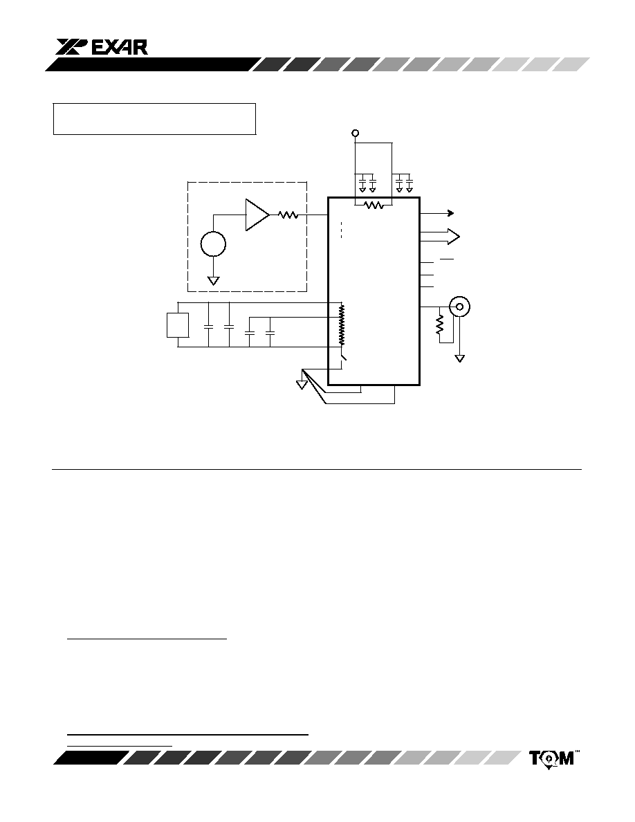
SIMPLIFIED BLOCK AND TIMING DIAGRAM
OFW
10
DFF
N
N
CLK
Ladder
Fine
Com-
Adder
4
5
6
CLK
1/2 R
B
AGND DGND
Coarse
Comparators
N
OFW
Resolution
parators
N-1
N-1
AV
DD
DV
DD
V
REF(+)
V
REF1(≠)
DB9-DB0
DB9-DB0
1 or 4
MUX
A
IN1
A
IN4
S
2 to 4
Decoder
A1
A0
WR
A
IN2
A
IN3
PD
V
REF(≠)
4
Latch
B
S
PIN CONFIGURATIONS
See Packaging Section for
Package Dimensions
28 Pin SOIC (Jedec, 0.300") ≠ S28
28 Pin SSOP ≠ A28
DB2
DB1
DB0
PD
AGND
1/2 R
AV
DD
A
IN4
V
REF(≠)
V
REF(+)
DGND
A1
A0
CLK
DB8
DV
DD
DB3
DB4
DB5
DB6
DB7
28
1
15
14
2
3
4
5
6
7
17
16
8
9
19
18
10
11
23
22
21
20
27
26
25
24
12
13
DB9
OFW
A
IN3
A
IN2
A
IN1
V
REF1(≠)
WR
13
16
14
15
1
2
3
4
5
6
7
8
9
10
28
27
26
25
24
23
22
21
20
19
11
18
12
17
DB2
DB1
DB0
PD
AGND
1/2 R
AV
DD
A
IN4
V
REF(≠)
V
REF(+)
DGND
A1
A0
CLK
DB8
DV
DD
DB3
DB4
DB5
DB6
DB7
DB9
OFW
A
IN3
A
IN2
A
IN1
V
REF1(≠)
WR
28 Pin PDIP (0.300")
NN28

MP8798
3
Rev. 3.00
PIN OUT DEFINITIONS
1
DB3
Data Output Bit 3
2
DB4
Data Output Bit 4
3
DB5
Data Output Bit 5
4
DB6
Data Output Bit 6
5
DB7
Data Output Bit 7
6
DGND
Digital Ground
7
DV
DD
Digital V
DD
8
WR
Write (Active Low)
9
A1
Address 1 Input
10
A0
Address 0 Input
11
CLK
Clock Input
12
DB8
Data Output Bit 8
13
DB9
Data Output Bit 9 (MSB)
14
OFW
Overflow Output
PIN NO.
NAME
DESCRIPTION
15
V
REF(+)
Upper Reference Voltage
16
V
REF(≠)
Lower Reference Voltage
17
V
REF1(≠)
Lower Reference Voltage
18
1/2 R
Reference Ladder Tap
19
A
IN1
Analog Signal Input 1
20
A
IN2
Analog Signal Input 2
21
A
IN3
Analog Signal Input 3
22
A
IN4
Analog Signal Input 4
23
AGND
Analog Ground
24
AV
DD
Analog V
DD
25
PD
Power Down
26
DB0
Data Output Bit 0 (LSB)
27
DB1
Data Output Bit 1
28
DB2
Data Output Bit 2
PIN NO.
NAME
DESCRIPTION
TRUTH TABLE FOR INPUT CHANNEL SELECTION
0
0
0
A
IN1
0
0
1
A
IN2
0
1
0
A
IN3
0
1
1
A
IN4
1
X
X
Previous selection
WR
A1
SELECTED ANALOG INPUT
A0
Note: WR, A1, A0 are internally connected to GND through
500k
resistance.

MP8798
4
Rev. 3.00
ELECTRICAL CHARACTERISTICS TABLE
Unless Otherwise Specified: AV
DD
= DV
DD
= 5 V, F
S
= 1 MHz (50% Duty Cycle),
V
REF(+)
= 4.6, V
REF(≠)
= AGND, T
A
= 25
∞
C
25
∞
C
Parameter
Symbol
Min
Typ
Max
Units
Test Conditions/Comments
KEY FEATURES
Resolution
10
Bits
Sampling Rate
F
S
.001
1
MHz
For Rated Performance
ACCURACY
2
Differential Non-Linearity
DNL
3/4
1
LSB
Integral Non-Linearity
INL
2
LSB
Best Fit Line
(Max INL ≠ Min INL)/2
Zero Scale Error
EZS
+0.50
LSB
Reference from V
REF(+)
to V
REF(≠)
Full Scale Error
EFS
≠2.5
LSB
REFERENCE VOLTAGES
Positive Ref. Voltage
V
REF(+)
AV
DD
V
Negative Ref. Voltage
V
REF(≠)
AGND
V
Differential Ref. Voltage
5
D
V
REF
0.5
AV
DD
V
Ladder Resistance
R
L
525
675
900
Ladder Temp. Coefficient
1
R
TCO
2000
ppm/
∞
C
Ladder Switch Resistance
1
12
Ladder Switch Off Leakage
1
I
LKG-SW
50
nA
ANALOG INPUT
1
Input Bandwidth
100
kHz
Input Voltage Range
7
V
IN
V
REF(≠)
V
REF(+)
V
Input Capacitance
3
C
IN
60
pF
Aperture Delay
t
AP
35
45
ns
DIGITAL INPUTS
Logical "1" Voltage
V
IH
2.0
V
Logical "0" Voltage
V
IL
0.8
V
Leakage Currents
I
IN
V
IN
=DGND to DV
DD
CLK
100
µ
A
PD, (Internal Res to DGND)
≠5
30
µ
A
Input Capacitance
5
pF
Clock Timing (
See NO TAG)
1
Clock Period
T
S
1000
ns
Rise & Fall Time
4
t
R
, t
F
10
ns
"High" Time
6
t
B
250
500,000
ns
"Low" Time
6
t
S
150
500,000
ns

MP8798
5
Rev. 3.00
ELECTRICAL CHARACTERISTICS TABLE (CONT'D)
25
∞
C
Specifications are subject to change without notice
Parameter
Symbol
Min
Typ
Max
Units
Test Conditions/Comments
DIGITAL OUTPUTS
C
OUT
=15 pF
Logical "1" Voltage
V
OH
DV
DD
-0.5
V
I
LOAD
= 2 mA
Logical "0" Voltage
V
OL
0.4
V
I
LOAD
= 4 mA
Tristate Leakage
I
OZ
0
5
µ
A
V
OUT
= 0 to DV
DD
Data Hold Time (
See NO TAG)
1
t
HLD
30
35
ns
Data Valid Delay
1
t
DL
35
45
ns
Write Pulse Width
1
t
WR
40
ns
Multiplexer Address Setup Time
1
t
AS
80
ns
Multiplexer Address Hold Time
1
t
AH
0
ns
Delay from WR to Multiplexer
1
Enable
t
MUXEN1
80
ns
Power Down Time
1
t
PD
300
ns
Power Up Time
1
t
PU
200
ns
POWER SUPPLIES
8
Power Down (I
DD
)
I
PD-DD
0.6
1.2
mA
Operating Voltage (AV
DD
, DV
DD
)
V
DD
4
5
6.5
V
Current (AV
DD
+ DV
DD
)
I
DD
6
10
mA
V
IN
= 2 V
NOTES:
1
Guaranteed. Not tested.
2
Tester measures code transition voltages by dithering the voltage of the analog input (V
IN
). The difference between the measured
code width and the ideal value (V
REF
/1024) is the DNL error (
see NO TAG). The INL error is the maximum distance (in LSBs) from
the best fit line to any transition voltage (
See Figure 7.).
3
See V
IN
input equivalent circuit (
see Figure 9.).
4
Clock specification to meet aperture specification (t
AP
). Actual rise/fall time can be less stringent with no loss of accuracy.
5
Specified values guarantee functional device. Refer to other parameters for accuracy.
6
System can clock MP8798 with any duty cycle as long as all timing conditions are met.
7
Input range where input is converted correctly into binary code. Input voltage outside specified range converts to zero or full scale
output.
8
DV
DD
and AV
DD
are connected through the silicon substrate. Connect together at the package.
ABSOLUTE MAXIMUM RATINGS (T
A
= +25
∞
C unless otherwise noted)
1, 2
V
DD
(to GND)
+7 V
. . . . . . . . . . . . . . . . . . . . . . . . . . . . . . . . . . .
V
REF(+)
& V
REF(≠)
GND ≠0.5 to V
DD
+0.5 V
. . . . . . . . . . . . . .
V
IN
GND ≠0.5 to V
DD
+0.5 V
. . . . . . . . . . . . . . . . . . . . . . . . . .
All Inputs
GND ≠0.5 to V
DD
+0.5 V
. . . . . . . . . . . . . . . . . . . . .
All Outputs
GND ≠0.5 to V
DD
+0.5 V
. . . . . . . . . . . . . . . . . . .
Storage Temperature
≠65 to +150
∞
C
. . . . . . . . . . . . . . . . . . .
Lead Temperature (Soldering 10 seconds)
+300
∞
C
. . . . . . .
Package Power Dissipation Rating to 75
∞
C
SOIC, PDIP
1000mW
. . . . . . . . . . . . . . . . . . . . . . . . . . . . .
Derates above 75
∞
C
14mW/
∞
C
. . . . . . . . . . . . . . . . . . . . .
NOTES:
1
Stresses above those listed under "Absolute Maximum Ratings" may cause permanent damage to the device. This is a
stress rating only and functional operation at or above this specification is not implied. Exposure to maximum rating
conditions for extended periods may affect device reliability.
2
Any input pin which can see a value outside the absolute maximum ratings
should be protected by Schottky diode clamps
(HP5082-2835) from input pin to the supplies.
All inputs have protection diodes which will protect the device from short
transients outside the supplies of less than 100mA for less than 100
µ
s.
3
V
DD
refers to AV
DD
and DV
DD
. GND refers to AGND and DGND.

MP8798
6
Rev. 3.00
AUTO
BALANCE
CLOCK
DATA
ANALOG
INPUT
SAMPLE
N≠1
Figure 1. MP8798 Timing Diagram
SAMPLE
N
SAMPLE
N+1
AUTO
BALANCE
N-1
T
S
V
IH
V
IL
V
OH
V
OL
t
F
t
B
t
R
t
S
t
DL
t
HLD
THEORY OF OPERATION
Analog-to-Digital Conversion
The MP8798 converts analog voltages into 1024 digital
codes by encoding the outputs of 15 coarse and 67 fine compa-
rators. Digital logic is used to generate the overflow bit. The con-
version is synchronous with the clock and it is accomplished in 2
clock periods.
The reference resistance ladder is a series of 1025 resistors.
The first and the last resistor of the ladder are half the value of
the others so that the following relations apply:
R
REF
= 1024
R V
REF
= V
REF(+)
≠ V
REF(≠)
= 1024
LSB
The clock signal generates the two internal phases,
B
(CLK
high) and
S
(CLK low = sample) (
See Figure 2.). The rising
edge of the CLK input marks the end of the sampling phase (
S
).
Internal delay of the clock circuitry will delay the actual instant
when
S
disconnects the latches from the comparators. This de-
lay is called aperture delay (t
AP
).
The coarse comparators make the first pass conversion and
selects a ladder range for the fine comparators. The fine compa-
rators are connected to the selected range during the next
B
phase.
Figure 2. MP8798 Comparators
S
B
B
S
Latch
Ref
Ladder
COARSE COMPARATOR
S
S
B
B
Latch
Selected
Range
FINE COMPARATOR
V
IN
V
IN
V
TAP
V
TAP
A
IN
Sampling, Ladder Sampling, and Conversion Timing
Figure 3. shows this relationship as a timing chart. A
IN
sam-
pling, ladder sampling and output data relationships are shown
for the general case where the levels which drive the ladder
need to change for each sampled A
IN
time point. The ladder is
referenced for both last A
IN
sample and next A
IN
sample at the
same time. If the ladder's levels change by more than 1 LSB,
one of the samples must be discarded. Also note that the clock
low period for the discarded A
IN
can be reduced to the minimum
t
S
time of 150 ns.
Figure 3. A
IN
Sampling, Ladder Sampling & Conversion Timing
Settle by Clock Update Time
Reference Stable Time ≠ For Sample A
IN
1
Sample A
IN
1
Reference Stable Time ≠ For Sample A
IN
2
Hold Reference Value Past
Clock Change for t
AP
Time
Short Cycle Sample will be discarded
Sample A
IN
2
A
IN
X1
Not Used
A
IN
X0
Sample A
IN
1
A
IN
X1
Sample A
IN
2
Sample Ladder
for A
IN
1
Sample Ladder
for A
IN
X1
Sample Ladder
for A
IN
2
Sample Ladder
for A
IN
X2
Compare Ladder
V/S A
IN
X0
Compare Ladder
V/S A
IN
1
Compare Ladder
V/S A
IN
X1
Compare Ladder
V/S A
IN
2
DATA A
IN
0
DATA A
IN
X0
DATA A
IN
1
DATA A
IN
X1
Not Used
Not Used
DATA
Ladder Compare
(LSB Bank)
Ladder Sample
Window (MSB Bank)
A
IN
Sample
Window
Clock
Update
References
External
Internal
External
t
S
F
B
F
S
F
B
F
S
F
B
F
S

MP8798
7
Rev. 3.00
Accuracy of Conversion: DNL and INL
The transfer function for an ideal A/D converter is shown in
Figure 4.
Figure 4. Ideal A/D Transfer Function
3FF
3FE
3FD
V
REF(≠)
V
REF(+)
DIGITAL
CODES
000
002
LSB
OFW = 0
V
0.5
LSB
0.5
LSB
001
OFW = 1
1 LSB
V001
V002
V
3FE
V
3FF
V
0FW
The overflow transition (V
OFW
) takes place at:
V
IN
= V
OFW
= V
REF(+)
≠ 0.5
LSB
The first and the last transitions for the data bits take place at:
V
IN
= V001 = V
REF(≠)
+ 0.5
LSB
V
IN
= V
3FF
= V
REF(+)
≠ 1.5
LSB
LSB = V
REF
/ 1024 = (V
3FF
≠ V001) / 1022
Note that the overflow transition is a flag and has no impact on
the data bits.
In a "real" converter the code-to-code transitions don't fall
exactly every V
REF
/1024 volts.
A positive DNL (Differential Non-Linearity) error means that
the real width of a particular code is larger than 1 LSB. This error
is measured in fractions of LSBs.
A Max DNL specification guarantees that ALL code widths
(DNL errors) are within the stated value. A specification of Max
DNL = + 0.5 LSB means that all code widths are within 0.5 and
1.5 LSB. If V
REF
= 4.608 V then 1 LSB = 4.5 mV and every code
width is within 2.25 and 6.75 mV.
N + 1
N
N ≠ 1
Output
Codes
Analog
Input
(N+1) Code Width = V
(N+1)
≠ V
(N)
LSB = [ V
REF(+)
≠ V
REF(≠)
] / 1024
DNL
(N)
= [ V
(N+1)
≠ V
(N)
] ≠ LSB
Figure 5. DNL Measurement
On Production Tester
LSB
DNL
V
(N+1)
V
(N)
The formulas for Differential Non-linearity (DNL), Integral
Non-Linearity (INL) and zero and full scale errors (E
ZS
, E
FS
) are:
DNL (001) = V002 ≠ V001 ≠ LSB
: : :
DNL (3FE) = V
3FF
≠ V
3FE
≠ LSB
E
FS
(full scale error) = V
3FF
≠ [V
REF(+)
≠1.5
LSB]
E
ZS
(zero scale error) = V
001
≠ [V
REF(≠)
+ 0.5
LSB]
Figure 6. Real A/D Transfer Curve
DIGITAL
CODES
0.5
LSB
000
001
002
3FE
3FF
V
1.5
LSB
V001
V002
V
3FE
V
3FF
V
REF(≠)
V
REF(+)
E
ZS
E
FS
Figure 6. shows the zero scale and full scale error terms.

MP8798
8
Rev. 3.00
Figure 7. gives a visual definition of the INL error. The chart
shows a 3-bit converter transfer curve with greatly exaggerated
DNL errors to show the deviation of the real transfer curve from
the ideal one.
After a tester has measured all the transition voltages, the
computer draws a line parallel to the ideal transfer line. By defi-
nition the best fit line makes equal the positive and the negative
INL errors. For example, an INL error of ≠1 to +2 LSB's relative
to the Ideal Line would be +1.5 LSB's relative to the best fit line.
7
6
5
4
3
2
1
Figure 7. INL Error Calculation
Output
Codes
Analog Input (Volt)
Best Fit Line
EFS
EZS
LSB
Ideal Transfer Line
Real Transfer Line
INL
Clock and Conversion Timing
A system will clock the MP8798 continuously or it will give
clock pulses intermittently when a conversion is desired. The
timing of
Figure 8a shows normal operation, while the timing of
Figure 8b keeps the MP8798 in balance and ready to sample the
analog input.
Figure 8. Relationship of Data to Clock
CLOCK
DATA
b. Single sampling
N
N
BALANCE
CLOCK
DATA
a. Continuous sampling
N
N+1
N
N+1
Analog Input
The MP8798 has very flexible input range characteristics.
The user may set V
REF(+)
and V
REF(≠)
to two fixed voltages and
then vary the input DC and AC levels to match the V
REF
range.
Another method is to first design the analog input circuitry and
then adjust the reference voltages for the analog input range.
One advantage is that this approach may eliminate the need for
external gain and offset adjust circuitry which may be required
by fixed input range A/Ds.
The MP8798's performance is optimized by using analog in-
put circuitry that is capable of driving the A
IN
input.
Figure 9.
shows the equivalent circuit for A
IN
.
300
15 pF
Figure 9. Analog Input Equivalent Circuit
V
DD
A
IN
40
S
60 pF
87 pF
160
4
1 pF
10 pF
Channel
Selection
4
Control
R Series
40
R MUX
500
87 pF
1/2 [ V
REF(+)
+ V
REF(≠)
]
S
B
4 pF
+

MP8798
9
Rev. 3.00
Analog Input Multiplexer
The MP8798 includes a 4-channel analog input multiplexer.
The relationship between the clock, the multiplexer address, the
WR and the output data is shown in
Figure 10.
WR
Clock
DB0-DB9
…………………………
…………………………
……
……
t
CLKS2
t
WR
t
CLKH2
Address
t
AS
t
AH
Sample N
Old Address
Sample M
New Address
Sample
M+1
N-2 Valid
N-1 Valid
Old Address
N Valid
Old Address
M Valid
New Address
Figure 10. MUX Address Timing
t
CLKS2
= t
CLKH2
= 0
A1, A0
MUXEN
(Internal Signal)
t
AS
t
AH
WR
t
WR
t
MUXEN1
Figure 11. Analog MUX Timing
Reference Voltages
The input/output relationship is a function of V
REF
:
A
IN
= V
IN
≠ V
REF(≠)
V
REF
= V
REF(+)
≠ V
REF(≠)
DATA = 1023
(A
IN
/V
REF
)
A system can increase total gain by reducing V
REF
.
Digital Interfaces
The logic encodes the outputs of the comparators into a bi-
nary code and latches the data in a D-type flip-flop for output.
The functional equivalent of the MP8798 (
Figure 12.) is com-
posed of:
1)
Delay stage (t
AP
) from the clock to the sampling phase
(
S
).
2)
An ideal analog switch which samples V
IN
.
3)
An ideal A/D which tracks and converts V
IN
with no
delay.
4)
A series of two DFF's with specified hold (t
HLD
) and
delay (t
DL
) times.
t
AP
, t
HLD
and t
DL
are specified in the Electrical Characteristics
table.
Figure 12. MP8798 Functional Equivalent
Circuit and Interface Timing
V
IN
S
A/D
MP8798
CLK
DB9-DB0
N
N+1
N-1
N
t
DL
t
HLD
D Q
D Q
DB9-DB0
CLK
V
IN
t
AP

MP8798
10
Rev. 3.00
Power Down
Figure 13. shows the relationship between the clock,
sampled A
IN
to output data relationship and the effect of power
down.
««««««
««««««
Figure 13. Power Down Timing Diagram
N-2 Valid
DB0-DB9
CLK
V
IN
PD
I
DD
, IV
REF(+)
SAMPLE
N
SAMPLE
M
SAMPLE
M+1
N-1 Valid
N Valid
M Valid
t
CLKS1
t
CLKH1
t
PD
t
PU
MP8798
11
Rev. 3.00
APPLICATION NOTES
Figure 14. Typical Circuit Connections
OFW
CLK
DB9 - DB0
AGND
DGND
(Substrate)
MP8798
A
IN1
V
REF(+)
V
REF(≠)
1/2 R
Buffer
AV
DD
DV
DD
C
1D,
C
2D
C
1A,
C
2A
C
1
= 4.7 or 10
µ
F Tantalum
C
2
= 0.1
µ
F Chip Cap or low inductance capacitor
R
T
= Clock Transmission Line Termination
Reference
Voltage
Source
V
REF1(≠)
A
IN
C
1
C
2
C
1
C
2
+
≠
+5 V
R
T
1 of 4
A
IN4
Z
100
W
Resistive
Isolation of
50 to 100
W
A0
A1
WR
The following information will be useful in maximizing the per-
formance of the MP8798.
1. All signals should not exceed AV
DD
+0.5 V or AGND ≠0.5 V
or DV
DD
+0.5 V or DGND ≠0.5 V.
2. Any input pin which can see a value outside the absolute
maximum ratings (AV
DD
or DV
DD
+0.5 V or AGND ≠0.5 V)
should be protected by diode clamps (HP5082-2835) from
input pin to the supplies. All MP8798 inputs have input pro-
tection diodes which will protect the device from short tran-
sients outside the supply ranges.
3. The design of a PC board will affect the accuracy of MP8798.
Use of wire wrap is not recommended.
4. The analog input signal (V
IN
) is quite sensitive and should be
properly routed and terminated. It should be shielded from
the clock and digital outputs so as to minimize cross coupling
and noise pickup.
5. The analog input should be driven by a low impedance (less
than 50
).
6. Analog and digital ground planes should be substantial and
common at one point only. The ground plane should act as a
shield for parasitics and not a return path for signals. To re-
duce noise levels, use separate low impedance ground
paths.
DGND should not be shared with other digital cir-
cuitry. If separate low impedance paths cannot be provided,
DGND should be connected to AGND next to the MP8798.
7.
DV
DD
should not be shared with other digital circuitry to
avoid conversion errors caused by digital supply transients.
DV
DD
for the MP8798 should be connected to AV
DD
next to
the MP8798.
8. DV
DD
and AV
DD
are connected inside the MP8798 through
the N ≠ doped silicon substrate. Any DC voltage difference
between DV
DD
and AV
DD
will cause undesirable internal
currents.
9. Each power supply and reference voltage pin should be
decoupled with a ceramic (0.1
µ
F) and a tantalum (10
µ
F) ca-
pacitor as close to the device as possible.
10. The digital output should not drive long wires. The capacitive
coupling and reflection will contribute noise to the conver-
sion. When driving distant loads, buffers should be used.
100
resistors in series with the digital outputs in some ap-
plications reduces the digital output disruption of A
IN
.

MP8798
12
Rev. 3.00
Figure 15. Example of a Reference Voltage Source
0.1
µ
F
MP5010
+5 V
+
≠
+
≠
5 k
100k
Figure 16.
5 V Analog Input
V
REF(+)
V
IN
+
≠
R
R
A
IN1
V
REF(≠)
5 V
+5 V
+5 V
DB0
AGND
AV
DD
For R = 5k use Beckman Instruments #694-3-R10k resistor array or equivalent.
NOTE: High R values affect the input BW of ADC due to the (R
C
IN
of ADC) time constant. Therefore, for different
applications the R value needs to be selected as a tradeoff between A
IN
settling time and power dissipation.
1 of 4
A
IN4
Figure 17.
10 V Analog Input
V
REF(+)
V
IN
+
≠
2R
R
A
IN1
V
REF(≠)
10 V
+5 V
+5 V
DB0
For R = 5k use Beckman Instruments #694-3-R10k resistor array or equivalent.
NOTE: High R values affect the input BW of ADC due to the (R
C
IN
of ADC) time constant. Therefore, for different
applications the R value needs to be selected as a tradeoff between A
IN
settling time and power dissipation.
2R
1 of 4
A
IN4
AGND
AV
DD

MP8798
13
Rev. 3.00
Figure 18. A/D Ladder and A
IN
with Programmed Control
(of V
REF(+),
V
REF(≠),
1/2 TAP.)
V
IN
+
≠
@ Power Down write values to DAC 3, 2, 1 = DAC 4 to minimize power consumption.
Only A
IN
and Ladder detail shown.
DAC4
DAC3
DAC1
MP8798
V
REF(+)
1/2
V
REF(+)
V
REF1(≠)
DAC MP7641
DAC8
DAC7
DAC6
DAC5
V
IN
+
≠
V
IN
+
≠
V
IN
+
≠
A
IN4
A
IN1
A
IN2
A
IN3
MP8798
14
Rev. 3.00
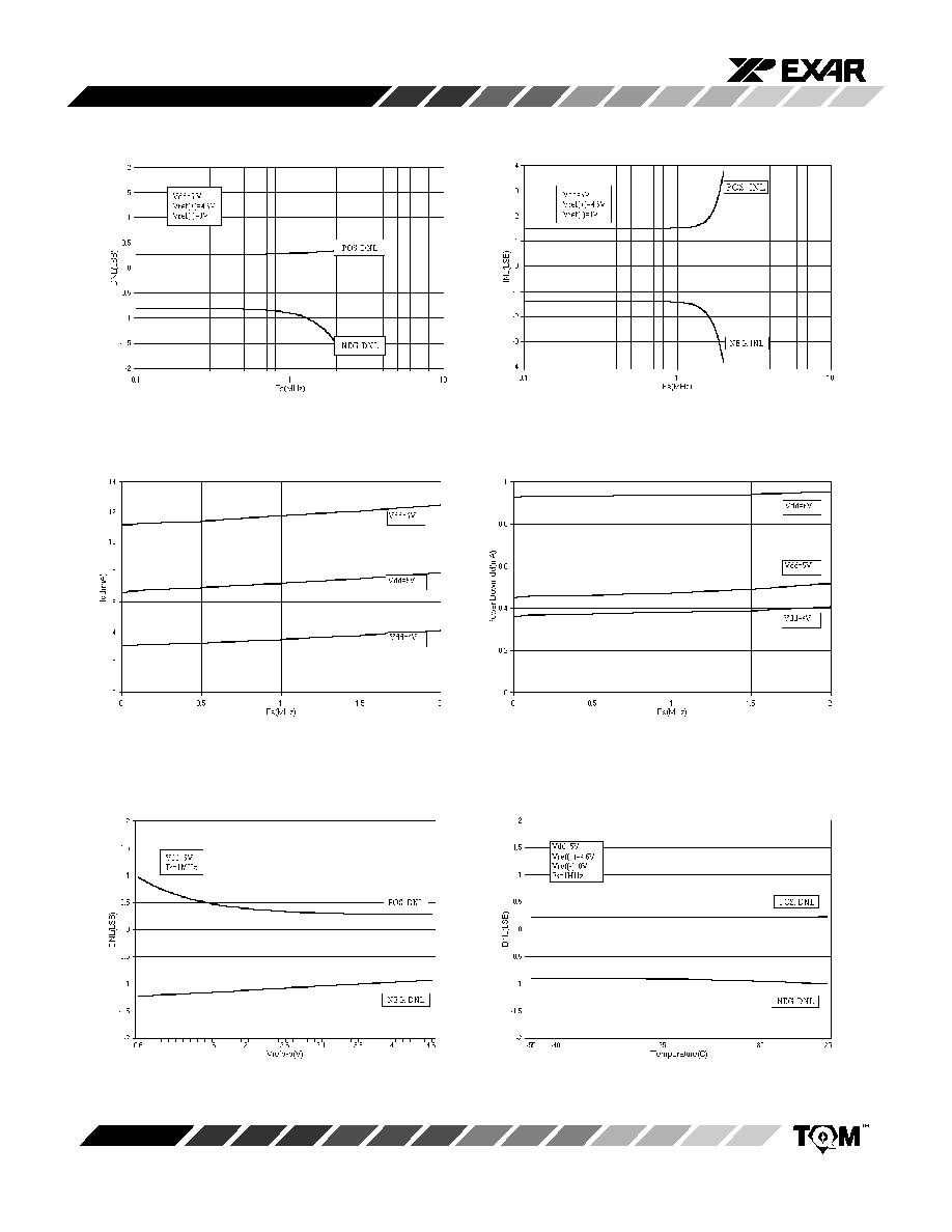
PERFORMANCE CHARACTERISTICS
Graph 1. DNL vs. Sampling Frequency
Graph 2. INL vs. Sampling Frequency
Graph 3. Supply Current vs.
Sampling Frequency
Graph 4. Power Down Current vs.
Sampling Frequency
Graph 5. DNL vs. Reference Voltage
Graph 6. DNL vs. Temperature

MP8798
15
Rev. 3.00
Graph 7. Supply Current vs.
Temperature
Graph 8. Power Down Current vs.
Temperature
Graph 9. Reference Resistance vs.
Temperature
MP8798
16
Rev. 3.00
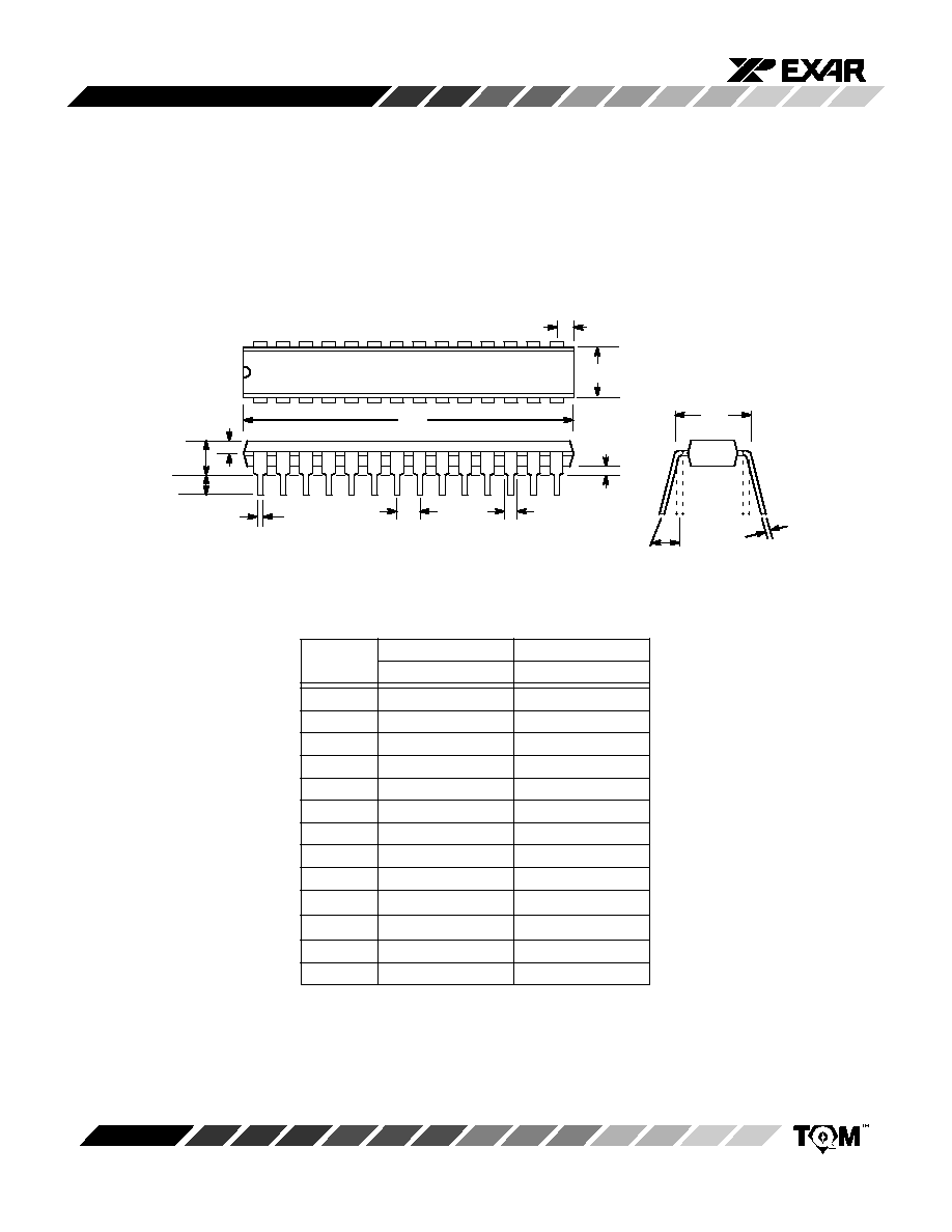
28 LEAD PLASTIC DUAL-IN-LINE
(300 MIL PDIP)
NN28
SYMBOL
MIN
MAX
MIN
MAX
INCHES
A
0.130
0.230
3.30
5.84
A
1
0.015
≠≠
0.381
≠≠
B
0.014
0.023
0.356
0.584
B
1
(1)
0.038
0.065
0.965
1.65
C
0.008
0.015
0.203
0.381
D
1.340
1.485
34.04
37.72
E
0.290
0.325
7.37
8.26
E
1
0.240
0.310
6.10
7.87
e
0.100 BSC
2.54 BSC
L
0.115
0.150
2.92
3.81
0
∞
15
∞
0
∞
15
∞
Q
1
0.055
0.070
1.40
1.78
S
0.020
0.100
0.508
2.54
MILLIMETERS
Note:
(1)
The minimum limit for dimensions B1 may be 0.023"
(0.58 mm) for all four corner leads only.
28
1
15
14
D
e
B
1
A
1
E
1
A
L
B
Q
1
Seating
Plane
C
E
S
MP8798
17
Rev. 3.00
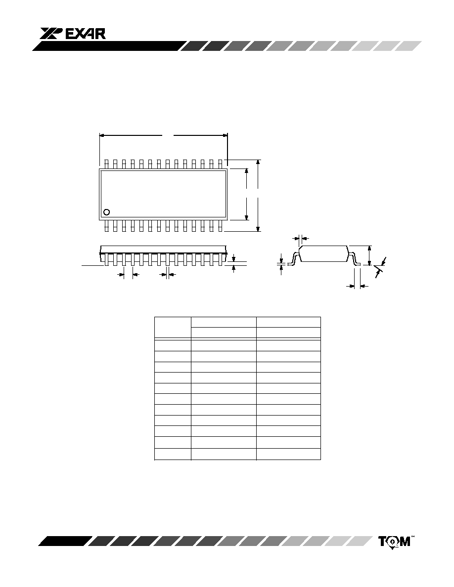
SYMBOL
MIN
MAX
MIN
MAX
A
0.097
0.104
2.464
2.642
A1
0.0050
0.0115
0.127
0.292
B
0.014
0.019
0.356
0.483
C
0.0091
0.0125
0.231
0.318
D
0.701
0.711
17.81
18.06
E
0.292
0.299
7.42
7.59
e
0.050 BSC
1.27 BSC
H
0.400
0.410
10.16
10.41
h
0.010
0.016
0.254
0.406
L
0.016
0.035
0.406
0.889
0
∞
8
∞
0
∞
8
∞
INCHES
MILLIMETERS
28 LEAD SMALL OUTLINE
(300 MIL JEDEC SOIC)
S28
e
D
E
H
B
A
L
C
A
1
Seating
Plane
h x 45
∞
28
15
14

MP8798
18
Rev. 3.00
SYMBOL
MIN
MAX
MIN
MAX
A
1.73
2.05
0.068
0.081
A
1
0.05
0.21
0.002
0.008
B
0.20
0.40
0.008
0.016
C
0.13
0.25
0.005
0.010
D
10.07
10.40
0.397
0.409
E
5.20
5.38
0.205
0.212
e
0.65 BSC
0.0256 BSC
H
7.65
8.1
0.301
0.319
L
0.45
0.95
0.018
0.037
0
∞
8
∞
0
∞
8
∞
INCHES
MILLIMETERS
28 LEAD SHRINK SMALL OUTLINE PACKAGE
(SSOP)
A28
e
D
E
H
B
A
L
C
A
1
Seating
Plane
28
15
14
1

MP8798
19
Rev. 3.00
Notes

MP8798
20
Rev. 3.00
NOTICE
EXAR Corporation reserves the right to make changes to the products contained in this publication in order to im-
prove design, performance or reliability. EXAR Corporation assumes no responsibility for the use of any circuits de-
scribed herein, conveys no license under any patent or other right, and makes no representation that the circuits are
free of patent infringement. Charts and schedules contains here in are only for illustration purposes and may vary
depending upon a user's specific application. While the information in this publication has been carefully checked;
no responsibility, however, is assumed for inaccuracies.
EXAR Corporation does not recommend the use of any of its products in life support applications where the failure or
malfunction of the product can reasonably be expected to cause failure of the life support system or to significantly
affect its safety or effectiveness. Products are not authorized for use in such applications unless EXAR Corporation
receives, in writing, assurances to its satisfaction that: (a) the risk of injury or damage has been minimized; (b) the
user assumes all such risks; (c) potential liability of EXAR Corporation is adequately protected under the circum-
stances.
Copyright 1993 EXAR Corporation
Datasheet April 1995
Reproduction, in part or whole, without the prior written consent of EXAR Corporation is prohibited.