 | –≠–ª–µ–∫—Ç—Ä–æ–Ω–Ω—ã–π –∫–æ–º–ø–æ–Ω–µ–Ω—Ç: MP8799AE | –°–∫–∞—á–∞—Ç—å:  PDF PDF  ZIP ZIP |

MP8799
1
Rev. 3.00
FEATURES
∑
10-Bit Resolution
∑
8-Channel Mux
∑
Sampling Rates from <1 kHz to 1 MHz
∑
Very Low Power CMOS - 30 mW (typ)
∑
Power Down; Lower Consumption ≠ 3 mW (typ)
∑
Input Range between GND and V
DD
∑
No S/H Required for Analog Signals less than 100 kHz
∑
No S/H Required for CCD Signals less than 1 MHz
∑
Single Power Supply (4 to 6 Volts)
∑
Latch-Up Free
∑
High ESD Protection: 4000 Volts Minimum
∑
3 V Version: MP87L99
CMOS
Very Low Power, 1 MSPS, 10-Bit
Analog-to-Digital Converter with 8-Channel Mux
BENEFITS
∑
Reduced Board Space (Small Package)
∑
Reduced External Parts, No Sample/Hold Needed
∑
Suitable for Battery & Power Critical Applications
∑
Designer can Adapt Input Range & Scaling
APPLICATIONS
∑ µ
P/DSP Interface and Control Applications
∑
High Resolution Imaging ≠ Scanners & Copiers
∑
Wireless Digital Communications
∑
Multiplexed Data Acquisition
GENERAL DESCRIPTION
The MP8799 is a flexible, easy to use, precision 10-bit
Analog-to-Digital Converter with 8-channel mux that operates
over a wide range of input and sampling conditions. The
MP8799 can operate with pulsed "on demand" conversion
operation or continuous "pipeline" operation for sampling rates
up to 1 MHz. The elimination of the S/H requirements, very low
power, and small package size offer the designer a low cost
solution. No sample and hold is required for charge couple
device applications up to 1 MHz, or multiplexed input
applications when the signal source bandwidth is limited to 100
kHz. The input architecture of the MP8799 allows direct
interface to any analog input range between AGND and AV
DD
(0
to 2 V, 1 to 4 V, 0 to 5 V, etc.). The user simply sets V
REF(+)
and
V
REF(≠)
to encompass the desired input range.
Scaled reference resistor tap @ 1/4 R, 1/2 R and 3/4 R allows
for customizing the transfer curve as well as providing a 1/2 span
reference voltage. Digital outputs are CMOS and TTL
compatible.
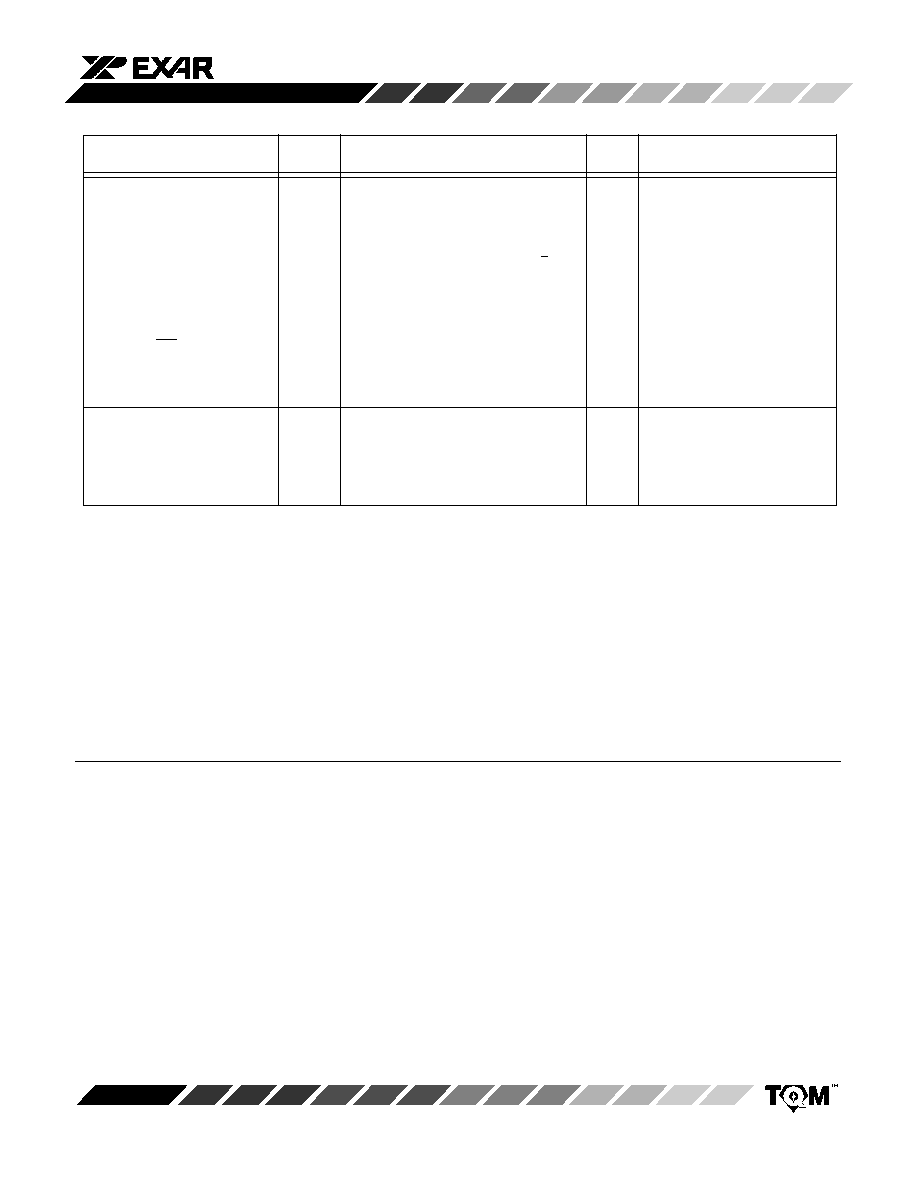
The MP8799 uses a two-step flash technique. The first
segment converts the 4 MSBs and consists of 15 autobalanced
comparators, latches, an encoder, and buffer storage registers.
The second segment converts the remaining 6 LSBs.
When the power down input is "high", the data outputs DB9 to
DB0 hold the current values and V
REF(≠)
is disconnected from
V
REF1(≠).
The power consumption during the power down mode
is approximately 3mW.
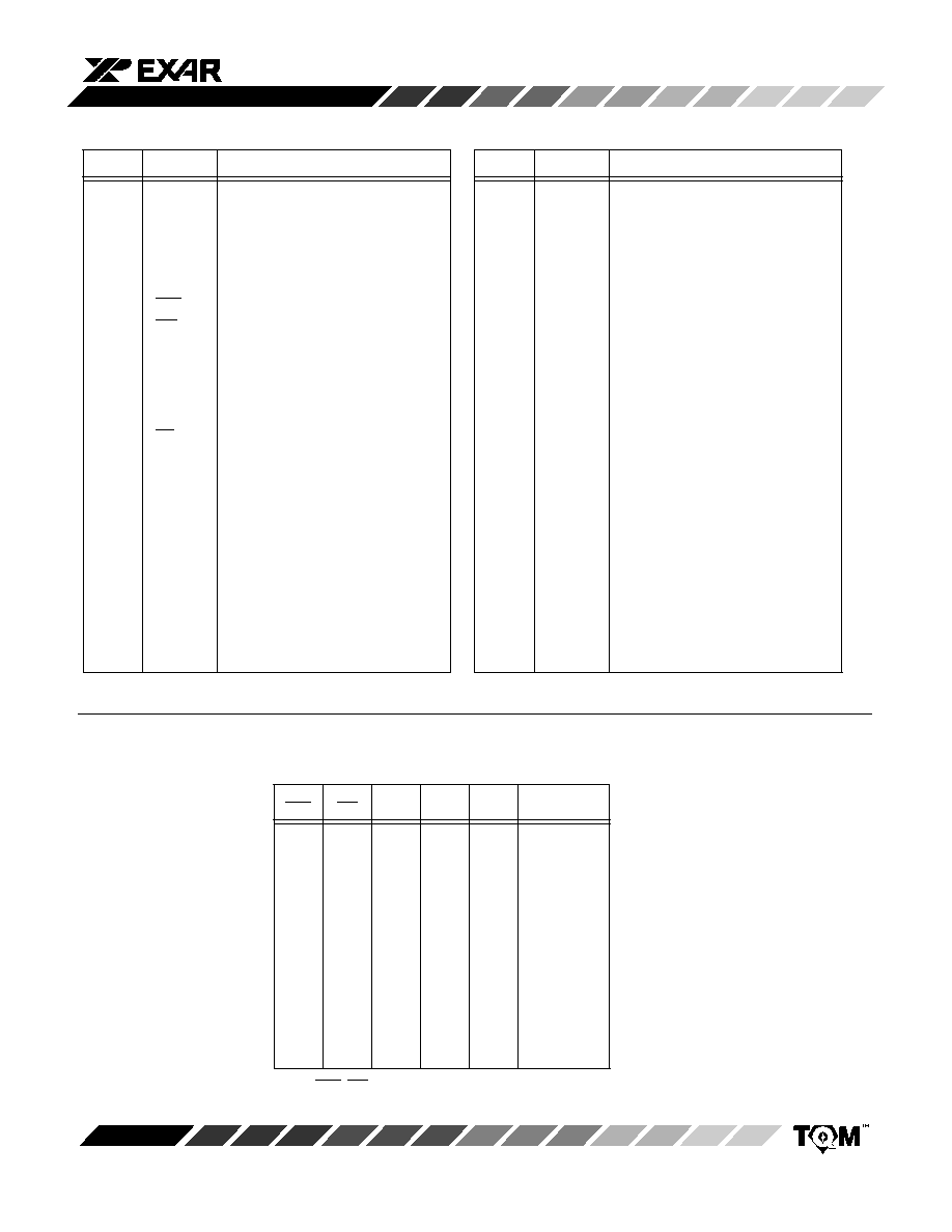
ORDERING INFORMATION
Package
Type
Temperature
Range
Part No.
DNL
(LSB)
INL
(LSB)
PQFP
≠40 to +85
∞
C
MP8799AE
1
2

MP8799
2
Rev. 3.00
SIMPLIFIED BLOCK AND TIMING DIAGRAM
OFW
10
DFF
N
N
CLK
Fine
Com-
Adder
4
5
6
CLK
R2
R1
B
DGND
Coarse
Comparators
N
OFW
Resolution
parators
N-1
N-1
AV
DD
DV
DD
V
REF(+)
DB9-DB0
DB9-DB0
1 or 8
MUX
A
IN1
A
IN8
S
3 to 8
Decoder
A1
A0
WR
AV
DD
OE
A2
CLR
AGND
V
REF1(≠)
PD
R3
Ladder
V
REF(≠)
Latch
8
B
S
PIN CONFIGURATIONS
See Packaging Section for
Package Dimensions
33
23
22
12
1
11
34
44
Index
44-Pin PQFP (10mm x 10mm)
QN44
See the following
page for pin numbers
and descriptions
MP8799
3
Rev. 3.00
PIN OUT DEFINITIONS
1
DB6
Data Output Bit 6
2
DB7
Data Output Bit 7
3
DGND
Digital Ground
4
DGND
Digital Ground
5
DV
DD
Digital V
DD
6
CLR
Clear (Active Low)
7
WR
Write (Active Low)
8
A2
Address 2
9
A1
Address 1
10
A0
Address 0
11
CLK
Clock Input
12
OE
Output Enable (Active Low)
13
N/C
No Connect
14
DB8
Data Output Bit 8
15
DB9
Data Output Bit 9 (MSB)
16
OFW
Overflow Output
17
V
REF(+)
Upper Reference Voltage
18
V
REF(≠)
Lower Reference Voltage
19
V
REF1(≠)
Lower Reference Voltage
20
R1
Reference Ladder Tap
21
R2
Reference Ladder Tap
22
A
IN8
Analog Signal Input 8
PIN NO.
NAME
DESCRIPTION
23
R3
Reference Ladder Tap
24
N/C
No Connect
25
A
IN1
Analog Signal Input 1
26
A
IN2
Analog Signal Input 2
27
A
IN3
Analog Signal Input 3
28
A
IN4
Analog Signal Input 4
29
A
IN5
Analog Signal Input 5
30
AGND
Analog Ground
31
AV
DD
Analog V
DD
32
AV
DD
Analog V
DD
33
A
IN6
Analog Signal Input 6
34
AGND
Analog Ground
35
PD
Power Down
36
A
IN7
Analog Signal Input 7
37
DB0
Data Output Bit 0 (LSB)
38
DB1
Data Output Bit 1
39
DB2
Data Output Bit 2
40
DB3
Data Output Bit 3
41
DB4
Data Output Bit 4
42
DB5
Data Output Bit 5
43
N/C
No Connect
44
N/C
No Connect
PIN NO.
NAME
DESCRIPTION
TRUTH TABLE FOR INPUT CHANNEL SELECTION
L
X
X
X
X
A
IN1
H
L
L
L
L
A
IN1
H
L
L
L
H
A
IN2
H
L
L
H
L
A
IN3
H
L
L
H
H
A
IN4
H
L
H
L
L
A
IN5
H
L
H
L
H
A
IN6
H
L
H
H
L
A
IN7
H
L
H
H
H
A
IN8
H
H
X
X
X
Previous
Selection
CLR
WR
A2
A1
A0
Selected
Analog Input
Note: CLR, WR, A2, A1, A0 are internally connected to
ground through 500k
resistance.

MP8799
4
Rev. 3.00
ELECTRICAL CHARACTERISTICS TABLE
Unless Otherwise Specified: AV
DD
= DV
DD
= 5 V, F
S
= 1 MHz (50% Duty Cycle),
V
REF(+)
= 4.6, V
REF(≠)
= AGND, T
A
= 25
∞
C
25
∞
C
Parameter
Symbol
Min
Typ
Max
Units
Test Conditions/Comments
KEY FEATURES
Resolution
10
Bits
Sampling Rate
F
S
.001
1
MHz
For Rated Performance
ACCURACY (A Grade)
2
Differential Non-Linearity
DNL
+1
LSB
LSB
Integral Non-Linearity
INL
2
LSB
Best Fit Line
(Max INL ≠ Min INL)/2
Zero Scale Error
EZS
+0.50
LSB
Reference from V
REF(+)
to V
REF(≠)
Full Scale Error
EFS
≠2.5
LSB
REFERENCE VOLTAGES
Positive Ref. Voltage
V
REF(+)
AV
DD
V
Negative Ref. Voltage
V
REF(≠)
AGND
V
Differential Ref. Voltage
5
V
REF
0.5
AV
DD
V
Ladder Resistance
R
L
525
675
900
Ladder Temp. Coefficient
1
R
TCO
2000
ppm/
∞
C
Ladder Switch Resistance
1
12
Ladder Switch Off Leakage
1
I
ILKG-SW
50
nA
ANALOG INPUT
1
Input Bandwidth
100
kHz
Input Voltage Range
7
V
IN
V
REF(≠)
V
REF(+)
V
Input Capacitance
3
C
IN
60
pF
Aperture Delay
t
AP
35
45
ns
DIGITAL INPUTS
Logical "1" Voltage
V
IH
2.0
V
Logical "0" Voltage
V
IL
0.8
V
Leakage Currents
I
IN
V
IN
=DGND to DV
DD
CLK
+100
µ
A
PD, OE (Internal Res to DGND)
≠5
30
µ
A
Input Capacitance
5
pF
Clock Timing (
See Figure 1.)
1
Clock Period
T
S
1000
ns
Rise & Fall Time
4
t
R
, t
F
10
ns
"High" Time
6
t
B
250
500,000
ns
"Low" Time
6
t
S
150
500,000
ns
MP8799
5
Rev. 3.00
ELECTRICAL CHARACTERISTICS TABLE (CONT'D)
25
∞
C
Specifications are subject to change without notice
Parameter
Symbol
Min
Typ
Max
Units
Test Conditions/Comments
DIGITAL OUTPUTS
C
OUT
=15 pF
Logical "1" Voltage
V
OH
DV
DD
-0.5
V
I
LOAD
= 2 mA
Logical "0" Voltage
V
OL
0.4
V
I
LOAD
= 4 mA
Tristate Leakage
I
OZ
0
+5
µ
A
V
OUT
= 0 to DV
DD
Data Hold Time (
See Figure 1.)
1
t
HLD
30
35
ns
Data Valid Delay
1
t
DL
35
45
ns
Write Pulse Width
1
t
WR
40
ns
Multiplexer Address Setup Time
1
t
AS
80
ns
Multiplexer Address Hold Time
1
t
AH
0
ns
Delay from WR to Multiplexer
1
Enable
t
MUXEN1
80
ns
Power Down Time
1
t
PD
300
ns
Power Up Time
1
t
PU
200
ns
POWER SUPPLIES
8
Power Down (I
DD
)
I
PD-DD
0.6
1.2
mA
Operating Voltage (AV
DD
, DV
DD
)
V
DD
4
5
6.5
V
Current (AV
DD
+ DV
DD
)
I
DD
6
10
mA
V
IN
= 2 V
NOTES:
1
Guaranteed. Not tested.
2
Tester measures code transition voltages by dithering the voltage of the analog input (V
IN
). The difference between the measured
code width and the ideal value (V
REF
/1024) is the DNL error (
see Figure 4.). The INL error is the maximum distance (in LSBs) from
the best fit line to any transition voltage (
See Figure 7.).
3
See V
IN
input equivalent circuit (
see Figure 9.).
4
Clock specification to meet aperture specification (t
AP
). Actual rise/fall time can be less stringent with no loss of accuracy.
5
Specified values guarantee functional device. Refer to other parameters for accuracy.
6
System can clock MP8799 with any duty cycle as long as all timing conditions are met.
7
Input range where input is converted correctly into binary code. Input voltage outside specified range converts to zero or full scale
output.
8
DV
DD
and AV
DD
are connected through the silicon substrate. Connect together at the package.
ABSOLUTE MAXIMUM RATINGS (T
A
= +25
∞
C unless otherwise noted)
1, 2, 3
V
DD
(to GND)
+7 V
. . . . . . . . . . . . . . . . . . . . . . . . . . . . . . . . . . .
V
REF(+)
, V
REF(≠),
V
REF1(≠)
GND ≠0.5 to V
DD
+0.5 V
. . . . . . .
All A
INs
GND ≠0.5 to V
DD
+0.5 V
. . . . . . . . . . . . . . . . . . . . . . .
All Inputs
GND ≠0.5 to V
DD
+0.5 V
. . . . . . . . . . . . . . . . . . . . .
All Outputs
GND ≠0.5 to V
DD
+0.5 V
. . . . . . . . . . . . . . . . . . .
Storage Temperature
≠65 to +150
∞
C
. . . . . . . . . . . . . . . . . . .
Lead Temperature (Soldering 10 seconds)
+300
∞
C
. . . . . . .
Package Power Dissipation Rating to 75
∞
C
PQFP
450mW
. . . . . . . . . . . . . . . . . . . . . . . . . . . . . . . . . . .
Derates above 75
∞
C
14mW/
∞
C
. . . . . . . . . . . . . . . . . . . . .
NOTES:
1
Stresses above those listed under "Absolute Maximum Ratings" may cause permanent damage to the device. This is a
stress rating only and functional operation at or above this specification is not implied. Exposure to maximum rating
conditions for extended periods may affect device reliability.
2
Any input pin which can see a value outside the absolute maximum ratings
should be protected by Schottky diode clamps
(HP5082-2835) from input pin to the supplies.
All inputs have protection diodes which will protect the device from short
transients outside the supplies of less than 100mA for less than 100
µ
s.
3
V
DD
refers to AV
DD
and DV
DD
. GND refers to AGND and DGND.