
ST34C87
...the analog plus company
TM
QUAD RS-422 CMOS
Differential Line Driver
Rev. 1.01
E
1991
EXAR Corporation, 48720 Kato Road, Fremont, CA 94538
z
(510) 668-7000
z
FAX (510) 668-7017
1
June 1997-3
FEATURES
D
Pin-to-Pin Compatible with National DS34C87
D
Low Power CMOS Design
D
Three-State Outputs with Enable Pin
D
Meets the EIA RS-422 Requirements
D
Low Propagation Delays
D
High Speed
GENERAL DESCRIPTION
The ST34C87 is a CMOS quad differential line driver
designed to meet the standard RS-422 requirements and
digital data transmission over balanced lines. To improve
noise margin and output stability for slow changing input
signals, special hysteresis is built in the ST34C87 circuit.
The ST34C87 is a high speed CMOS line driver designed
to operate with MFM / RLL controllers and hard disk
drives as well as RS-422 digital data transmission
applications. ST34C87 is suitable for low power 5V
operation with high input voltage protection devices.
ORDERING INFORMATION
Part No.
Package
Operating
Temperature Range
ST34C87CP16
16 Lead 300 Mil PDIP
0
∞
C to +70
∞
C
ST34C87CF16
16 Lead 150 Mil JEDEC SOIC
0
∞
C to +70
∞
C
ST34C87IP16
16 Lead 300 Mil PDIP
-40
∞
C to +85
∞
C
ST34C87IF16
16 Lead 150 Mil JEDEC SOIC
-40
∞
C to +85
∞
C
Figure 1. Block Diagram
INPUT A
OUTPUTA+
OUTPUT A-
ENABLE A/B
OUTPUTB-
OUTPUTB+
INPUT B
INPUT D
OUTPUT D+
OUTPUT D-
OUTPUT C-
OUTPUT C+
INPUT C
ENABLE C/D

ST34C87
2
Rev. 1.01
PIN CONFIGURATION
16 Lead PDIP (0.300")
V
CC
INPUT D
OUTPUT D+
OUTPUT D-
ENABLE C/D
OUTPUT C-
OUTPUT C+
INPUT C
INPUT A
OUTPUT A+
OUTPUT A-
ENABLE A/B
OUTPUT B-
OUTPUT B+
INPUT B
GND
1
2
3
4
5
6
7
8
16
15
14
13
12
11
10
9
16 Lead SOIC (Jedec, 0.150")
16
1
9
8
2
3
4
5
6
7
15
14
13
12
11
10
V
CC
INPUT D
OUTPUT D+
OUTPUT D-
OUTPUT C-
OUTPUT C+
INPUT C
INPUT A
OUTPUT A+
OUTPUT A-
OUTPUT B-
OUTPUT B+
INPUT B
GND
ENABLE C/D
ENABLE A/B
PIN DESCRIPTION
Pin #
Symbol
Type
Description
1
INPUT A
I
Driver A input pin.
2
OUTPUT
A+
O
Driver A differential non-inverting output pin.
3
OUTPUT
A-
O
Driver A differential inverting output pin.
4
ENABLE
A/B
I
Gate control (active high). This pin is one of the two control pins which enables or disables all
four drivers. All four drivers are gated with two input or gate.
5
OUTPUT
B-
O
Driver B differential inverting output pin.
6
OUTPUT
B+
O
Driver B differential non-inverting output pin.
7
INPUT B
I
Driver B input pin.
8
GND
O
Signal and power ground.
9
INPUT C
I
Driver C input pin.
10
OUTPUT
C+
O
Driver C differential non-inverting output pin.
11
OUTPUT
C-
O
Driver C differential inverting output pin.
12
ENABLE
C/D
I
Gate control (active low). See ENABLE A/B pin description.
13
OUTPUT
D-
O
Driver D differential inverting output pin.
14
OUTPUT
D+
O
Driver D differential non-inverting output pin.
15
INPUT D
I
Driver D input pin.
16
V
CC
I
Power supply pin.
ST34C87
3
Rev. 1.01
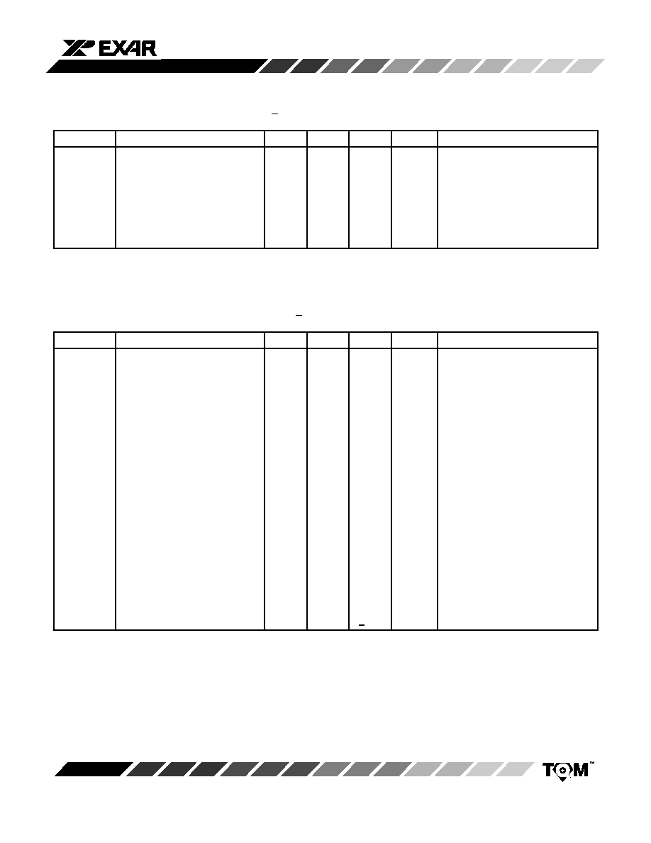
AC ELECTRICAL CHARACTERISTICS
Test Conditions: -40
∞
C - +85
∞
C, V
CC
= 5.0V + 10% unless otherwise specified.
Symbol
Parameter
Min.
Typ.
Max.
Unit
Conditions
T
1
Propagation Delay, Input to
Output
8
10
ns
S1 open
T
2
Differential Output Rise and Fall
Time
8
10
ns
S1 open
T
3
Output Enable Time
18
20
ns
S1 close
T
4
Output Disable Time
18
20
ns
S1 close
T
5
1
Skew
2
ns
S1 open
Note:
1
Skew is defined as the difference in propagation delays between complementary outputs at the 50% point.
DC ELECTRICAL CHARACTERISTICS
Test Conditions: T
A
= -40
∞
C - +85
∞
C, V
CC
= 5.0V + 10% unless otherwise specified.
Symbol
Parameter
Min.
Typ.
Max.
Unit
Conditions
I
IN
Input Current
+
1.0
m
A
I
CC
Operating Current
600
m
A
I
OZ
Three-State Output Leakage
+2.0
m
A
V
IH
Input High Level
2.0
V
V
IL
Input Low Level
0.8
V
V
OH
Output High Level
2.5
V
V
OL
Output Low Level
0.5
V
V
OS
Differential Output Level
2.0
V
R
L
=100
W
V
OC
Common Mode Output Voltage
3.0
V
R
L
=100
W
V
OD
Difference in Common Mode
Output
0.4
R
L
=100
W
C
IN
Input Capacitance
7
10
15
pF
C
PD
Power Dissipation Capacitance
100
pF
I
OS
Output Short Current
-200
-30
mA
V
I
N
=V
CC
or GND
I
OFF
Output Leakage Current Power
Off
100
m
A
V
OUT
=6V
-100
m
A
V
OUT
=0.25V
I
DC
Output Current
+150
mA
Specifications are subject to change without notice

ST34C87
4
Rev. 1.01
ABSOLUTE MAXIMUM RATINGS
Supply Range
7V
. . . . . . . . . . . . . . . . . . . . . . . . . . . . . . .
Voltage at Any Pin
GND-0.3V to V
CC
+ 0.3V
. . . . . . . .
Operating Temperature
≠40
∞
C to +85
∞
C
. . . . . . . . . . .
Storage Temperature
-60
∞
C to +160
∞
C
. . . . . . . . . . . .
Package Dissipation
500mW
. . . . . . . . . . . . . . . . . . . . .
Enable
A/B
C/D
Output
Differential
Non-Inverting
Output
Differential
Inverting
Output
L
X
Z
Z
H
L
L
H
H
H
H
L
X = Don't care
Z = Three-State (high impedance)
Table 1. Functional Table
Figure 2. Test Condition
V
CC
R3
S1
500
R2
50
C3
40pF
C2
40pF
C1
40pF
Driver
U1
ENABLE
Input
R1
50

ST34C87
5
Rev. 1.01
ENABLE
ENABLE*
INPUT X
OUTPUT X+
OUTPUT X-
T
3
T
3
T
4
T
4
T
1
T
1
T
1
T
1
T
2
T
2
90%
10%
90%
10%
OUTPUT X+
OUTPUT X-
T
5
50%
50%
Figure 4. Differential Line Driver Timing

ST34C87
6
Rev. 1.01
16 LEAD PLASTIC DUAL-IN-LINE
(300 MIL PDIP)
Rev. 1.00
16
1
9
8
D
e
B
1
A
1
E
1
E
A
L
B
Seating
Plane
SYMBOL
MIN
MAX
MIN
MAX
INCHES
A
0.145
0.210
3.68
5.33
A
1
0.015
0.070
0.38
1.78
A
2
0.115
0.195
2.92
4.95
B
0.014
0.024
0.36
0.56
B
1
0.030
0.070
0.76
1.78
C
0.008
0.014
0.20
0.38
D
0.745
0.840
18.92
21.34
E
0.300
0.325
7.62
8.26
E
1
0.240
0.280
6.10
7.11
e
0.100 BSC
2.54 BSC
e
A
0.300 BSC
7.62 BSC
e
B
0.310
0.430
7.87
10.92
L
0.115
0.160
2.92
4.06
0
∞
15
∞
0
∞
15
∞
MILLIMETERS
A
2
C
Note: The control dimension is the inch column
e
B
e
A

ST34C87
7
Rev. 1.01
SYMBOL
MIN
MAX
MIN
MAX
A
0.053
0.069
1.35
1.75
A
1
0.004
0.010
0.10
0.25
B
0.013
0.020
0.33
0.51
C
0.007
0.010
0.19
0.25
D
0.386
0.394
9.80
10.00
E
0.150
0.157
3.80
4.00
e
0.050 BSC
1.27 BSC
H
0.228
0.244
5.80
6.20
L
0.016
0.050
0.40
1.27
0
∞
8
∞
0
∞
8
∞
INCHES
MILLIMETERS
16 LEAD SMALL OUTLINE
(150 MIL JEDEC SOIC)
Rev. 1.00
e
16
9
8
D
E
H
B
A
L
C
A
1
Seating
Plane
Note: The control dimension is the millimeter column
1

ST34C87
8
Rev. 1.01
NOTICE
EXAR Corporation reserves the right to make changes to the products contained in this publication in order to im-
prove design, performance or reliability. EXAR Corporation assumes no responsibility for the use of any circuits de-
scribed herein, conveys no license under any patent or other right, and makes no representation that the circuits are
free of patent infringement. Charts and schedules contained here in are only for illustration purposes and may vary
depending upon a user's specific application. While the information in this publication has been carefully checked;
no responsibility, however, is assumed for inaccuracies.
EXAR Corporation does not recommend the use of any of its products in life support applications where the failure or
malfunction of the product can reasonably be expected to cause failure of the life support system or to significantly
affect its safety or effectiveness. Products are not authorized for use in such applications unless EXAR Corporation
receives, in writing, assurances to its satisfaction that: (a) the risk of injury or damage has been minimized; (b) the
user assumes all such risks; (c) potential liability of EXAR Corporation is adequately protected under the circum-
stances.
Copyright 1997 EXAR Corporation
Datasheet June 1997
Reproduction, in part or whole, without the prior written consent of EXAR Corporation is prohibited.