
EXAR Corporation, 48720 Kato Road, Fremont, CA 94538
∑
(510) 668-7000
∑
FAX (510) 668-7017
ST49C101A-XX
High Frequency Clock Multiplier
January 1999 -3
Rev. 2.20
FEATURES
∑
Mask Programmable Analog Phase Locked
Loop
∑
Up to 200MHz Operation
∑
Preprogrammed Multiplication Factors of 2, 3, 4, 5,
6, 8, 10 and 12X
∑
Low Output Jitter
∑
Replace Expensive High Frequency Oscillator
∑
Crystal Oscillator Circuit On Chip
∑
Low Power Single Supply 5V or 3.3V CMOS
Technology
∑
Small 8 Lead SOIC Package
GENERAL DESCRIPTION
The ST49C101A-XX is a mask programmable mono-
lithic analog phase locked loop device, designed to
replace existing high frequency crystal oscillator with
a low frequency crystal. The high performance
APPLICATIONS
∑
Voltage Controlled Crystal Oscillator (VCXO)
∑
System Clock Multiplication in:
∑
Computer Systems
∑
Telecommunications Systems
∑
Set-top Boxes
ST49C101A-XX provides low jitter clock output and
operates up to 180 MHz. at 3.3 volts power supply. The
ST49C101A-XX supports preprogrammed multiplica-
tion factors of 2,3,4,5,6,8,10 and 12X.
ORDERING INFORMATION
.
r
e
b
m
u
N
t
r
a
P
e
g
a
k
c
a
P
g
n
i
t
a
r
e
p
O
e
g
n
a
R
e
r
u
t
a
r
e
p
m
e
T
1
0
-
8
F
C
A
1
0
1
C
9
4
T
S
C
I
O
S
c
e
d
e
J
li
M
0
5
1
d
a
e
L
8
0
o
0
7
o
t
C
o
C
3
0
-
8
F
C
A
1
0
1
C
9
4
T
S
C
I
O
S
c
e
d
e
J
li
M
0
5
1
d
a
e
L
8
0
o
0
7
o
t
C
o
C
5
0
-
8
F
C
A
1
0
1
C
9
4
T
S
C
I
O
S
c
e
d
e
J
li
M
0
5
1
d
a
e
L
8
0
o
0
7
o
t
C
o
C
6
0
-
8
F
C
A
1
0
1
C
9
4
T
S
C
I
O
S
c
e
d
e
J
li
M
0
5
1
d
a
e
L
8
0
o
0
7
o
t
C
o
C
7
0
-
8
F
C
A
1
0
1
C
9
4
T
S
C
I
O
S
c
e
d
e
J
li
M
0
5
1
d
a
e
L
8
0
o
0
7
o
t
C
o
C
8
0
-
8
F
C
A
1
0
1
C
9
4
T
S
C
I
O
S
c
e
d
e
J
li
M
0
5
1
d
a
e
L
8
0
o
0
7
o
t
C
o
C
9
0
-
8
F
C
A
1
0
1
C
9
4
T
S
C
I
O
S
c
e
d
e
J
li
M
0
5
1
d
a
e
L
8
0
o
0
7
o
t
C
o
C
0
1
-
8
F
C
A
1
0
1
C
9
4
T
S
C
I
O
S
c
e
d
e
J
li
M
0
5
1
d
a
e
L
8
0
o
0
7
o
t
C
o
C
3
1
-
8
F
C
A
1
0
1
C
9
4
T
S
C
I
O
S
c
e
d
e
J
li
M
0
5
1
d
a
e
L
8
0
o
0
7
o
t
C
o
C
5
1
-
8
F
C
A
1
0
1
C
9
4
T
S
C
I
O
S
c
e
d
e
J
li
M
0
5
1
d
a
e
L
8
0
o
0
7
o
t
C
o
C
y
r
o
t
c
a
F
tl
u
s
n
o
C
e
i
D
0
o
0
7
o
t
C
o
C
ST49C101A-XX
2
Rev. 2.20
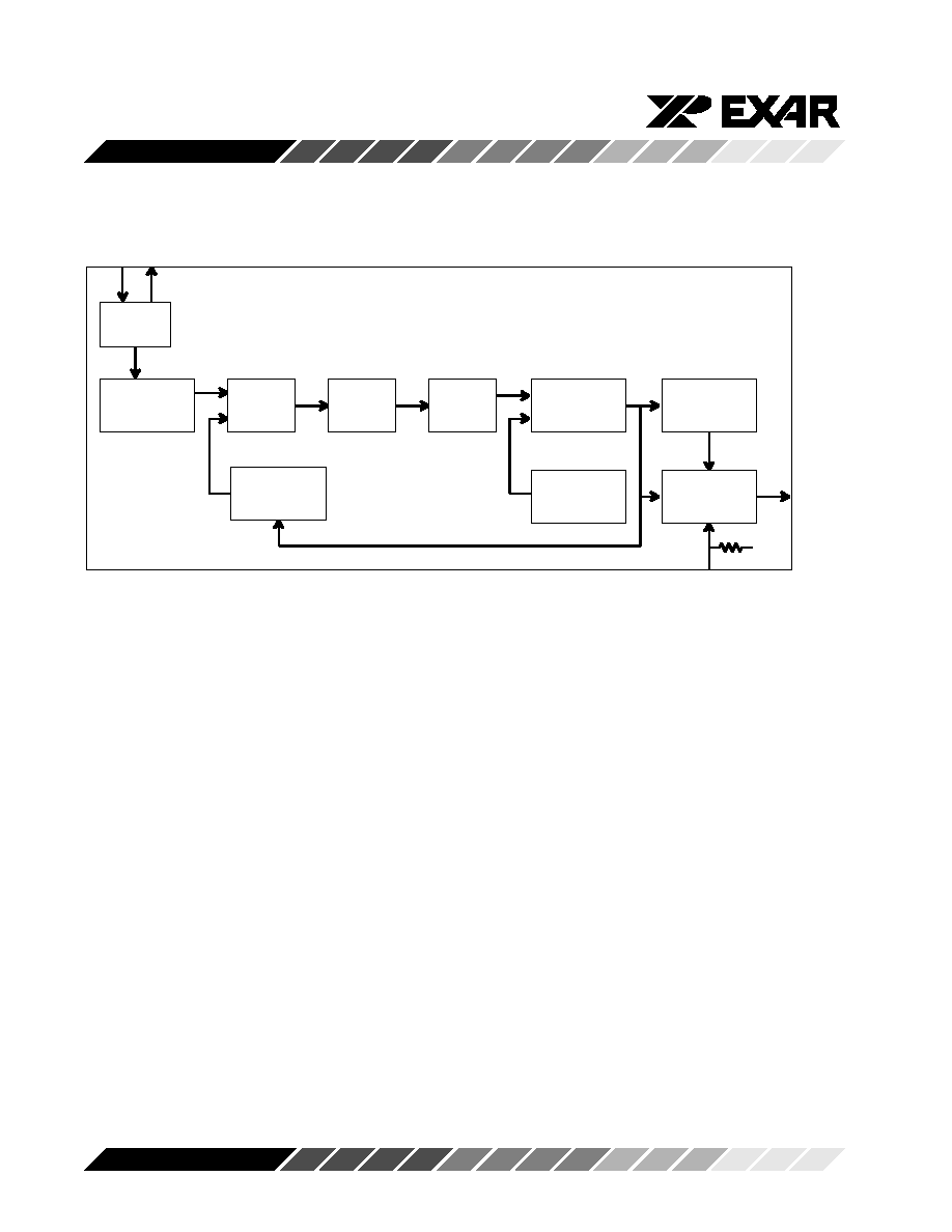
Oscillator
Circuit
Programmable
Counter
B
Phase
Detector
Charge
Pump
Loop
Filter
Voltage
Controlled
Oscillator
Programmable
Counter
C
Voltage
Reference
Circuit
Output
Buffer
Programmable
Counter
A
CLOCK
XTAL1
XTAL2
OE
VCC
Figure 1. Block Diagram

ST49C101A-XX
3
Rev. 2.20
PIN DESCRIPTION
Pin #
Symbol
Type
Description
1
XTAL1
I
Crystal or External Clock Input. A crystal can be connected to this pin
and XTAL2 pin to generate internal phase locked loop reference clock.
For external clock, XTAL2 is left open or used as buffered clock output.
2
1
OE
I
Clock Output Enable (Active high). CLOCK output is three stated when
this pin is low. Connect to DVCC for normal operation.
3
AGND
O
Analog Ground.
4
DGND
O
Digital Ground.
5
CLOCK
O
Programmed Output Clock.
6
DV
CC
I
Positive Supply Voltage. Single +5 or 3.3 volts.
7
AV
CC
I
Analog Supply Voltage. Single +5 or 3.3 volts.
8
XTAL2
O
Crystal Output.
Note:
1
Has internal weak pull-up resistor
8
1
5
4
2
3
7
6
X T A L 2
A V C C
D V C C
C L O C K
X T A L 1
O E
A G N D
D G N D
8 Pin SOIC (Jedec, 0.150")

ST49C101A-XX
4
Rev. 2.20
MULTIPLICATION FACTOR AND OUTPUT FRE-
QUENCY SELECTION
The ST49C101A-XX contains an analog phase locked
loop (PLL) circuit with digital closed loop dividers and
a final output divider to achieve the desired dividing
ratios for the clock output. The preprogrammed multi-
plication factor and output frequency are shown on
Table 1. The accuracy of the output frequency pro-
duced by the ST49C101A-XX depends on its input
frequency and multiplication factor.
APPLICATIONS
Two application examples are shown in Figure 2 and 3.
Figure 2 shows a lower cost high frequency crystal
oscillator circuit using the ST49C101-xx to increase
the fundamental crystal frequency. The crystal Y1 is
connected to XTAL1 and XTAL2 pins to use the
internal oscillator circuit. The oscillator provides the
reference clock to the PLL circuit for clock rate multi-
plication. Figure 3 shows a similar circuit using
external clock input on XTAL1 pin instead.
If a sinewave is used for external clock, it may be
necessary to AC couple the signal with a 0.047uF
capacitor to XTAL1 pin so that the internal circuitry
can establish the proper bias. Also, keep the peak-to-
peak signal, at XTAL pin, above ground level (AGND)
and below AVCC.
As a general board layout rule, it is recommended to
use two 0.01
µ
F bypass capacitors on DVCC and
AVCC power supply pins, and put them as closely as
possible to the chip.
Notes
1
See AC electrical characteristics for maximum operating
frequency.
X
X
-
A
1
0
1
C
9
4
T
S
r
o
t
c
a
F
t
u
p
t
u
O
.
x
a
M
y
c
n
e
u
q
e
r
F
1
C
C
V
1
1
0
-
A
1
0
1
C
9
4
T
S
2
1
z
H
M
0
0
2
z
H
M
0
4
1
V
0
.
5
V
3
.
3
3
0
-
A
1
0
1
C
9
4
T
S
8
z
H
M
0
0
2
z
H
M
0
4
1
V
0
.
5
V
3
.
3
5
0
-
A
1
0
1
C
9
4
T
S
6
z
H
M
0
0
2
z
H
M
0
4
1
V
0
.
5
V
3
.
3
6
0
-
A
1
0
1
C
9
4
T
S
4
z
H
M
0
2
1
r
o
0
.
5
V
3
.
3
7
0
-
A
1
0
1
C
9
4
T
S
3
z
H
M
0
8
z
H
M
0
7
V
0
.
5
V
3
.
3
8
0
-
A
1
0
1
C
9
4
T
S
2
z
H
M
0
8
z
H
M
0
7
V
0
.
5
V
3
.
3
9
0
-
A
1
0
1
C
9
4
T
S
5
z
H
M
0
0
2
z
H
M
0
4
1
V
0
.
5
V
3
.
3
0
1
-
A
1
0
1
C
9
4
T
S
0
1
z
H
M
0
8
1
V
3
.
3
3
1
-
A
1
0
1
C
9
4
T
S
8
z
H
M
0
8
1
V
3
.
3
5
1
-
A
1
0
1
C
9
4
T
S
6
z
H
M
0
8
1
V
3
.
3
Table 1. Preprogrammed Options

ST49C101A-XX
5
Rev. 2.20
XTAL1
XTAL2
AGND DGND
CLOCK
OE
U1
ST49C101A-XX
C1
C2
Y1
DGND
AGND
AGND
DGND
CLOCK= Xtal Freq. x Option
1
8
3
4
7
6
5
2
Parallel Cut
Fundamental
Resonance
20-30pF Load
Crystal
0.01uF
0.01uF
DVCC
DVCC
AVCC
DVCC
AVCC
Figure 2. High Frequency Crystal Oscillator Using a Crystal for Reference.
CLKin
XTAL1
XTAL2
CLOCK
OE
C2
U1
ST49C101A-XX
CLOCK = CLKin x Option
AGND
DGND
1
8
3
4
7
6
5
2
0.01uF
DVCC
AVCC
DVCC
AGND
DGND
AGND
DGND
DVCC
AVCC
C1
0.01uF
Figure 3. High Frequency Clock Rate Multiplication Using External Clock.

ST49C101A-XX
6
Rev. 2.20
DC ELECTRICAL CHARACTERISTICS
Test Conditions: T
A
= 25
∞
C, V
CC
= 5.0V + 10%, Operating Temperature Range 0
∞
C to 70
∞
C Unless
Otherwise Specified
Symbol
Parameter
Min.
Typ.
Max.
Unit
Conditions
V
IL
Input Low Level
0.8
V
V
IH
Input High Level
2.0
V
V
OL
Output Low Level
0.5
V
I
OL
= 8.0 mA
V
OH
Output High Level
2.8
V
I
OH
= 8.0 mA
I
IL
Input Low Current
-100
µ
A
OE Pin only
I
IH
Input High Current
1
µ
A
V
IN
=V
CC,
OE Pin only
I
CC
Operating Current
35
50
mA
No Load. CLOCK=100MHz
R
IN
Input Pull-up Resistance
75
110
155
k
AC ELECTRICAL CHARACTERISTICS
Test Conditions: T
A
= 25
∞
C, V
CC
= 5.0V + 10%, Operating Temperature Range 0
∞
C to 70
∞
C Unless
Otherwise Specified
Symbol
Parameter
Min.
Typ.
Max.
Unit
Conditions
T1,T2
CLOCK Rise/Fall Time
1.5
3
ns
Load=30 pF, 0.2 V
CC
- 0.8 V
CC
T4
T4 + T5
Duty Cycle
45
50
55
%
V
CC
/2 Switch Point Up To 100MHz,
Load = 20pF
T4
T4 + T5
Duty Cycle
40
50
60
%
V
CC
/2 Switch Point 100-150MHz, 95
(AC Terminated)
T3
Jitter 1 Sigma
+0.4
+1
%
Of Period
T3
Jitter Absolute
+1
+3
%
Of Period
T
IN
Input Reference Frequency
12
20
30
MHz
T
OUT
Output Frequency
50
200
MHz
ST49C101A-01
50
200
MHz
ST49C101A-03
50
200
MHz
ST49C101A-05
50
120
MHz
ST49C101A-06
25
80
MHz
ST49C101A-07
25
80
MHz
ST49C101A-08
50
200
MHz
ST49C101A-09

ST49C101A-XX
7
Rev. 2.20
DC ELECTRICAL CHARACTERISTICS
Test Conditions: T
A
= 25
∞
C, V
CC
=3.3V +/- 10%, Operating Temperature Range 0
∞
C to 70
∞
C Unless
Otherwise Specified
Symbol
Parameter
Min.
Typ.
Max.
Unit
Conditions
V
IL
Input Low Level
0.8
V
V
IH
Input High Level
2.0
V
V
OL
Output Low Level
0.5
V
I
OL
= 4.0mA
V
OH
Output High Level
2.0
V
I
OH
= 4.0mA
I
IL
Input Low Current
-100
µ
A
OE Pin Only
II
H
Input High Current
1
µ
A
V
IN
=VCC
,
OE Pin only
I
CC
Operating Current
22
40
mA
No Load. CLOCK=100MHz
R
IN
Input Pull≠up Resistance
75
110
155
k
AC ELECTRICAL CHARACTERISTICS
Test Conditions: T
A
= 25
∞
C, V
CC
=3.3V +/- 10%, Operating Temperature Range 0
∞
C to 70
∞
C Unless
Otherwise Specified
Symbol
Parameter
Min.
Typ.
Max.
Unit
Conditions
T1, T2
CLOCK Rise/Fall Time
2
4
ns
Load = 30 pF, 0.2 V
CC
- 0.8 V
CC
T4
T4+T5
Duty Cycle
45
50
55
%
V
CC
/2 switch point up to 100MHz,
Load = 30 pF
T4
T4+T5
Duty Cycle
40
50
60
%
V
CC
/2 switch point 100-150MHz, 95
(AC Terminated)
T3
Jitter 1 Sigma
+ 0.4
+ 1
%
Of Period
T3
Jitter Absolute
+ 1
+ 3
%
Of Period
T
IN
Input Reference Frequency
12
20
30
MHz
T
OUT
Output Frequency
50
140
MHz
ST49C101A-01
50
140
MHz
ST49C101A-03
50
140
MHz
ST49C101A-05
50
150
MHz
ST49C101A-05 at V
CC
=3.13V min.
50
120
MHz
ST49C101A-06
25
70
MHz
ST49C101A-07
25
70
MHz
ST49C101A-08
50
140
MHz
ST49C101A-09
25
180
MHz
ST49C101A-10 at V
CC
=3.13V min.
25
180
MHz
ST49C101A-13 at V
CC
=3.13V min.
25
180
MHz
ST49C101A-15 at V
CC
=3.13V min.

ST49C101A-XX
8
Rev. 2.20
ABSOLUTE MAXIMUM RATINGS
Supply Range
7 V
Voltage at Any Pin
GND-0.3V to V
CC
+0.3V
Operating Temperature
0
∞
C to +70
∞
C
Storage Temperature
-40
∞
C to +150
∞
C
Package Dissipation
500mW
T4
T5
T3
T2
T1
Output
Clock
Figure 4. Timing Diagram

ST49C101A-XX
9
Rev. 2.20

ST49C101A-XX
10
Rev. 2.20
NOTICE
EXAR Corporation reserves the right to make changes to the products contained in this publication in order to
improve design, performance or reliability. EXAR Corporation assumes no responsibility for the use of any
circuits described herein, conveys no license under any patent or other right, and makes no representation that
the circuits are free of patent infringement. Charts and schedules contained here in are only for illustration
purposes and may vary depending upon a user's specific application. While the information in this publication
has been carefully checked; no responsibility, however, is assumed for in accuracies.
EXAR Corporation does not recommend the use of any of its products in life support applications where the
failure or malfunction of the product can reasonably be expected to cause failure of the life support system or to
significantly affect its safety or effectiveness. Products are not authorized for use in such applications unless
EXAR Corporation receives, in writing, assurances to its satisfaction that: (a) the risk of injury or damage has
been minimized; (b) the user assumes all such risks; (c) potential liability of EXAR Corporation is adequately
protected under the circumstances.
Copyright 1999 EXAR Corporation
Datasheet January 1999
Reproduction, in part or whole, without the prior written consent of EXAR Corporation is prohibited.