
6-3
ST78C34
PLCC Package
GENERAL PURPOSE PARALLEL
PRINTER PORT WITH 83 BYTE FIFO
DESCRIPTION
The ST78C34 is a monolithic Bidirectional Parallel
port designed to operate as a general purpose I/O port.
It contains all the necessary input/output signals to be
configured as a CENTRONICS printer port.
The ST78C34 is a general purpose input/output con-
troller with 83 byte internal FIFO. FIFO operation can
be enabled or disabled. For CENTRONICS printer
operation, all registers are mapped to IBM printer port
registers.
The ST78C34 is designed to operate as normal
printer interface without any additional settings. Con-
tents of the FIFO will be cleared after reset or setting
the INIT pin to a low state. The auto FIFO operation
starts after the first -ACK is received from the printer.
Contents of the FIFO transfer to the printer at the
printer loading speed.
FEATURES
∑
83 bytes of printer output FIFO
∑
Bi-directional software parallel port
∑
Bi-directional I/O ports
∑
Register compatible to IBM XT, AT, compatible
386, 486
∑
Selectable interrupt polarity
∑
Selectable FIFO interrupts
ORDERING INFORMATION
Part number
Pin
Package
Operating temperature
ST78C34CJ44
44
PLCC
0∞ C to + 70∞ C
ST78C34CP40
40
PDip
0∞ C to + 70∞ C
ST78C34IJ44
44
PLCC
-40∞ C to + 85∞ C
ST78C34IP40
40
PDip
-40∞ C to + 85∞ C
Rev. 3.00
6
5
4
3
2
1
44
43
42
41
40
7
8
9
10
11
12
13
14
15
16
17
39
38
37
36
35
34
33
32
31
30
29
18
19
20
21
22
23
24
25
26
27
28
N.C.
INTSEL
D7
D6
D5
D4
D3
D2
D1
D0
N.C.
N.
C.
IN
T
XT
AL
1
XT
AL
2
-C
S
GND
RE
SE
T
-S
TR
O
B
E
-A
U
T
O
F
DX
IN
I
T
-
S
L
C
TIN
N.C.
PD7
PD6
PD5
PD4
PD3
PD2
PD1
PD0
GND
N.C.
N.
C.
PE
-A
C
K
BU
S
Y
SL
C
T
-
E
RRO
R
VC
C
-I
O
R
-I
O
W
A1
A0
ST78C34CJ44

6-4
ST78C34
Rev. 3.00
Plastic-DIP Package
Figure 1, PACKAGE DESCRIPTION, ST78C34
1
2
3
4
5
6
7
8
9
10
11
12
13
14
15
16
17
18
19
20
40
39
38
37
36
35
34
33
32
31
30
29
28
27
26
25
24
23
22
21
-ERROR
SLCT
BUSY
-ACK
PE
INTSEL
D7
D6
D5
D4
D3
D2
D1
D0
N.C.
INT
XTAL1
XTAL2
-CS
GND
VCC
-IOR
-IOW
A1
A0
N.C.
PD7
PD6
PD5
PD4
PD3
PD2
PD1
PD0
GND
-SLCTIN
INIT
-AUTOFDX
-STROBE
RESET
S
T
7
8
C
34C
P40
6-5
ST78C34
Rev. 3.00
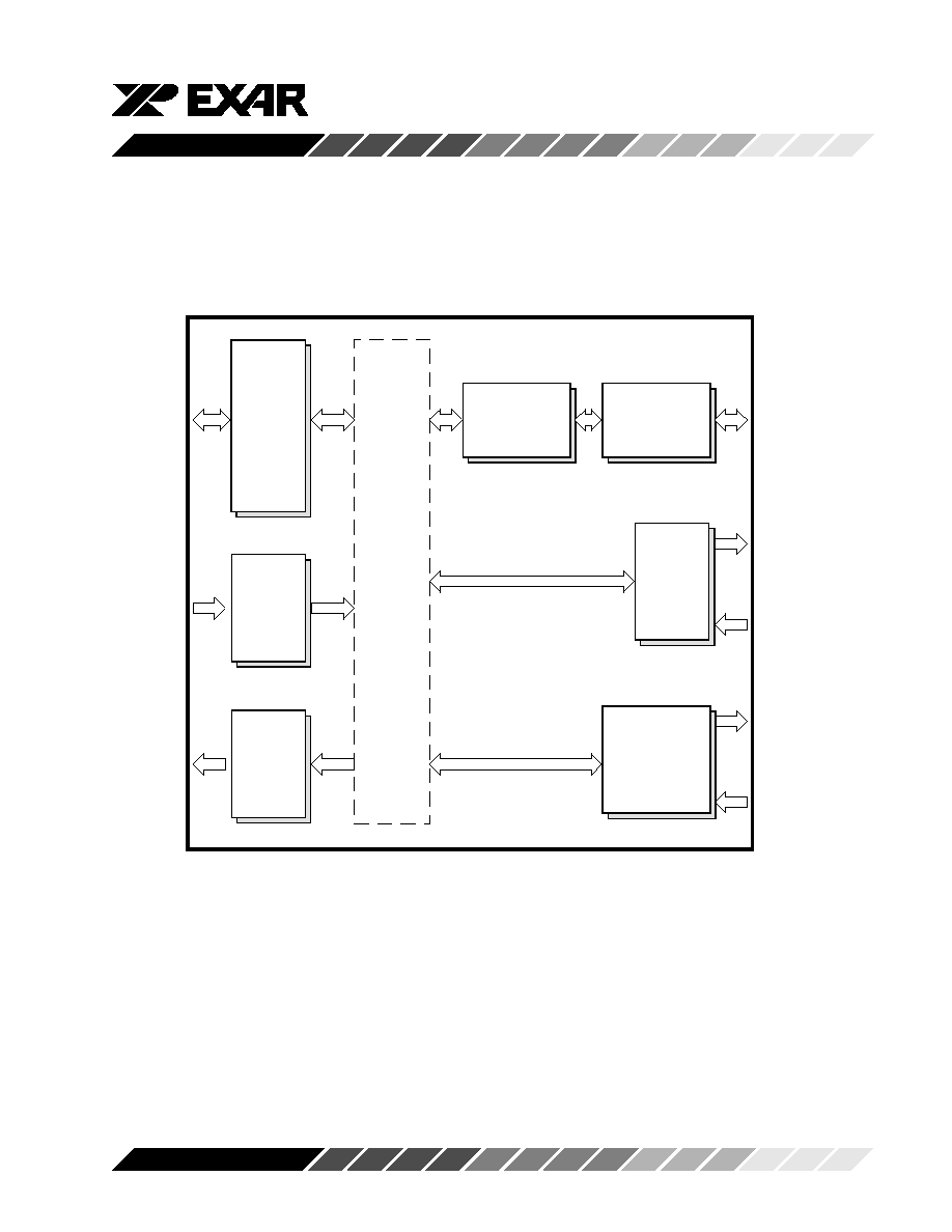
Figure 2, BLOCK DIAGRAM
D0-D7
-IOR
-IOW
RESET
A0-A1
-CS
INT
INTSEL
Data bu
s
&
C
o
n
t
rol Lo
gic
Re
g
i
st
er
S
e
l
ect
L
ogic
Int
err
u
p
t
Co
n
t
r
o
l
L
ogic
Printer
Data
Ports
PD0-PD7
Printer
Control
Logic
-STROBE
INIT
-AUTOFDX
-SELCTIN
PE, SELECT
BUSY, -ACK
-ERROR
Printer
FIFO
Registers
Int
er Co
n
n
ec
t
B
u
s
Li
n
e
s
&
C
o
n
t
rol s
i
gn
als
Clock
&
Timing
Generator
XTAL1
XTAL2

6-6
ST78C34
Rev. 3.00
SYMBOL DESCRIPTION
Symbol
Pin
Signal
Pin Description
40
44
type
-ERROR
1
1
I
General purpose input or line printer error (active low, with internal
pull-up). This is an output from the printer to indicate an error by
holding it low during error condition.
SLCT
2
2
I
General purpose input or line printer selected (active high, with
internal pull-up). This is an output from the printer to indicate that
the line printer has been selected.
BUSY
3
3
I
General purpose input or line printer busy (active high, with internal
pull-up). An output from the printer to indicate printer is not ready
to accept data.
-ACK
4
4
I
General purpose input or line printer acknowledge (active low, with
internal pull-up). An output from the printer to indicate that data has
been accepted successfully.
PE
5
5
I
General purpose input or line printer paper empty (active high, with
internal pull-up). An output from the printer to indicate out of paper.
INTSEL
6
8
I
Interrupt select mode. The external -ACK can be selected as an
interrupt source by connecting this pin to the VCC or left open.
Connecting this pin to GND will set the interrupt to latched mode,
reading the status register resets the INT output.
D0-D7
14-7
16-9
I/O
Bi-directional data bus. Eight bit, three state data bus to transfer
information to or from the CPU. D0 is the least significant bit of
the data bus.
INT
16
19
O
Interrupt output (selectable active low or high). To signal the state
of the printer port. This pin tracks the -ACK input pin, When -ACK
is low INT is low and when -ACK is high INT is high if selected as
active low interrupt.
XTAL1
17
20
I
Crystal input 1 or external clock input. A crystal can be connected
to this pin and XTAL2 pin to utilize the internal oscillator circuit. An
external clock can be used to clock oscillator circuit.
XTAL2
18
21
O
Crystal input 2 or buffered clock output. See XTAL1.
-CS
19
22
I
Chip select (active low). A low at this pin enables the ST78C34 /
CPU data transfer operation.

6-7
ST78C34
Rev. 3.00
SYMBOL DESCRIPTION
Symbol
Pin
Signal
Pin Description
40
44
type
GND
20
23
O
Signal and power ground.
RESET
21
24
I
Master reset (active high). A high on this pin will reset all the
outputs and internal registers.
-STROBE
22
25
I/O
General purpose I/O or strobe output (open drain active low, with
internal pull-up). To transfer latched data to the external peripheral
or printer.
-AUTOFDXT
23
26
I/O
General purpose I/O or line printer auto feed (open drain active
low, with internal pull-up). To signal the printer for continuous form
feed.
INIT
24
27
I/O
General purpose I/O or line printer initialize (open drain active
high, with internal pull-up). To signal the line printer to enter
internal initialization routine.
-SLCTIN
25
28
I/O
General purpose I/O or line printer select (open drain active low,
with internal pull-up). To select the line printer.
GND
26
30
O
Power and signal ground.
PD0-PD7
27-34
31-38
I/O
Bi-directional parallel ports (three state). To transfer data in or out
of the ST78C34 parallel port. PD7-PD0 are latched during output
mode.
A0-A1
36-37
40-41
I
Address lines. To select internal registers.
-IOW
38
42
I
Write strobe (active low). A low on this pin will transfer the contents
of the CPU data bus to the addressed register.
-IOR
39
43
I
Read strobe (active low). A low level on this pin transfers the
contents of the ST78C34 data bus to the CPU.
VCC
40
44
I
Power supply input.