 | ÐлекÑÑоннÑй компоненÑ: XR-2212CP | СкаÑаÑÑ:  PDF PDF  ZIP ZIP |
Äîêóìåíòàöèÿ è îïèñàíèÿ www.docs.chipfind.ru
XR-2212
...the analog plus company
TM
Precision
Phase-Locked Loop
Rev. 2.01
E
1979
EXAR Corporation, 48720 Kato Road, Fremont, CA 94538
z
(510) 668-7000
z
FAX (510) 668-7017
1
June 1997-3
FEATURES
D
Quadrature VCO Outputs
D
Wide Frequency Range (0.01Hz to 300kHz)
D
Wide Supply Voltage Range (4.5V to 20V)
D
TTL/HCMOS Compatible (V
CC
= 5VDC)
D
Wide Dynamic Range (2mV to 3Vrms)
D
Adjustable Tracking Range (
"
1% to
"
80%)
D
Excellent Temp. Stability 20ppm/
°
C, Typ.
APPLICATIONS
D
Frequency Synthesis
D
Data Synchronization
D
FM Detection
D
Tracking Filters
D
FSK Demodulation
GENERAL DESCRIPTION
The XR-2212 is an ultra-stable monolithic phase-locked
loop (PLL) system especially designed for data
communications and control system applications. Its on
board reference and uncommitted operational amplifier,
together with a typical temperature stability of better than
20ppm/
°
C, make it ideally suited for frequency synthesis,
FM detection, and tracking filter applications. The wide
input dynamic range, large operating voltage range, large
frequency range, and HCMOS and TTL compatibility
contribute to the usefulness and wide applicability of this
device.
ORDERING INFORMATION
Part No.
Package
Operating
Temperature Range
XR-2212M
16 Lead 300 Mil CDIP
-55
°
C to +125
°
C
XR-2212CP
16 Lead 300 Mil PDIP
0
°
C to +70
°
C
XR-2212P
16 Lead 300 Mil PDIP
-40
°
C to +85
°
C
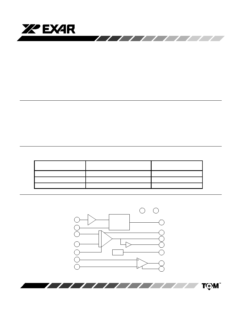
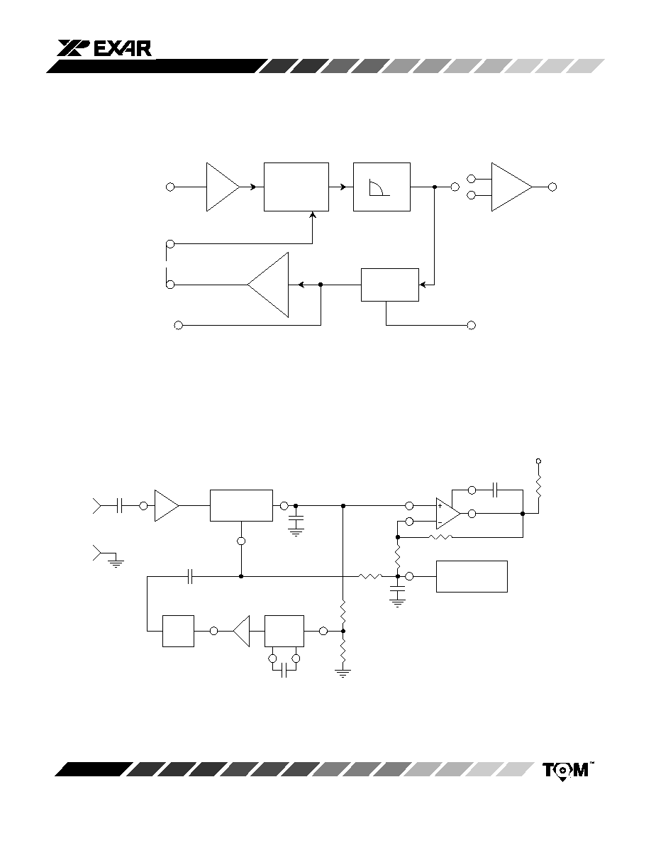
BLOCK DIAGRAM
2
INP
1
V
CC
4
GND
10
0-DET O
8
OUT
6
COMP
11
V
REF
5
VCOOV
3
VCOOC
15
VCOQO
12
TIM R
14
TIM C1
13
TIM C2
16
0-DET I
9
PINP
7
NINP
Figure 1. XR-2212 Block Diagram
Pre Amplifier
Phase
Detector
Op Amp
V
REF
Amp
VCO
XR-2212
2
Rev. 2.01
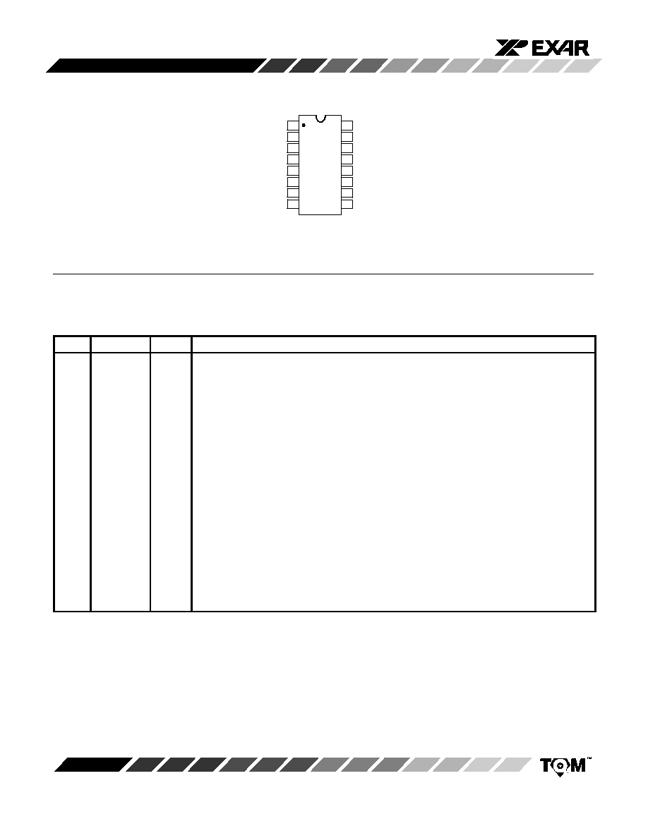
PIN CONFIGURATION
1
16 Lead PDIP, CDIP (0.300")
V
CC
INP
VCOOC
2
3
4
5
6
7
8
16
15
14
13
12
11
10
9
TIM R
TIM C2
TIM C1
VCOQO
0-DET I
GND
VCOOV
COMP
NINP
OUT
PINP
0-DET O
V
REF
PIN DESCRIPTION
Pin #
Symbol
Type
Description
1
V
CC
Positive Power Supply.
2
INP
I
Receive Analog Input.
3
VCOOC
O
VCO Current Output.
4
GND
Ground Pin.
5
VCOOV
O
VCO Voltage Source Output.
6
COMP
I
Uncommitted Amplifier, Frequency Compensation Input.
7
NINP
I
Inverted Input. Uncommitted amplifier.
8
OUT
O
Uncommitted Amplifier Output.
9
PINP
I
Positive Input. Uncommitted amplifier.
10
0-DET O
O
Phase Detector Output.
11
V
REF
O
Internal Voltage Reference. The value of V
REF
is V
CC
/2 -650mV.
12
TIM R
I
Timing Resistor Input. This pin connects to the timing resistor of the VCO.
13
TIM C2
I
Timing Capacitor Input. The timing capacitor connects between this pin and pin 14.
14
TIM C1
I
Timing Capacitor Input. The timing capacitor connects between this pin and pin 13.
15
VCOQO
O
VCO Quadrature Output.
16
0-DET I
I
Phase Detector Input.
XR-2212
3
Rev. 2.01
ELECTRICAL CHARACTERISTICS
Test Conditions: V
CC
= +12V, T
A
= + 25
°
C, R
0
= 30k
W
, C
0
= 0.033
m
F, unless otherwise specified. See
Figure 3 for component designation.
P
t
XR-2212M/2212P
XR-2212CP
U it
C
diti
Parameter
Min.
Typ.
Max.
Min.
Typ.
Max.
Units
Conditions
General Characteristics
Supply Voltage
4.5
15
4.5
15
V
Supply Current
6
10
6
12
mA
R
0
> 10k
W
., See
Figure 5
Oscillator Section
Frequency Accuracy
+1
+3
+1
%
Deviation from f
0
= 1/R
0
C
0
Frequency Stability
R
1
=
R
Temperature
1
+20
+50
+20
ppm/
°
C
See
Figure 9
Power Supply
0.05
0.5
0.05
%/V
V
CC
= 12 + 1V, See
Figure 8
0.2
0.2
%/V
V
CC
= 5 + 0.5V, See
Figure 8
Upper Frequency Limit
100
300
300
kHz
R
0
= 8.2k
W
, C
0
= 400pF
Lowest Practical Operating
F
0.01
0.01
Hz
R
0
= 2M
W
, C
0
= 50
m
F
Frequency
Timing Resistor, R
0
See
Figure 5
Operating Range
5
2000
5
2000
k
W
Recommended Range
15
100
15
100
k
W
See
Figure 8 and Figure 9
Oscillator Outputs
Voltage Output
Measured at Pin 5
Positive Swing, V
OH
11
11
V
Negative Swing, V
OL
0.4
0.8
0.5
V
Current Sink Capability
1
1
mA
Current Output
Measured at Pin 3
Peak Current Swing
100
150
150
m
A
Output Impedance
1
1
M
W
Quadrature Output
Measured at Pin 15
Output Swing
0.6
0.6
V
DC Level
0.3
0.3
V
Referenced to Pin 11
Output Impedance
3
3
k
W
Loop Phase Detector Section
Measured at Pin 10
Peak Output Current
+150
+200
+300
+100
+200
+300
m
A
Output Offset Current
+1
+2
m
A
Output Impedance
1
1
M
W
Maximum Swing
+4
+5
+4
+5
V
Referenced to Pin 11
Notes
1
For XR-2212P the parameters, although guaranteed over the recommended operating conditions, are not 100% tested in
production.
Bold face parameters are covered by production test and guaranteed over operating temperature range.
XR-2212
4
Rev. 2.01
ELECTRICAL CHARACTERISTICS
(CONT'D)
Parameter
XR-2212M/2212P
XR-2212CP
Units
Conditions
Parameter
Min.
Typ.
Max.
Min.
Typ.
Max.
Units
Conditions
Input Preamp Section
Measured at Pin 2
Input Impedance
20
20
k
W
Input Signal to Cause Limiting
2
10
2
mV rms
Op Amp Section
Voltage Gain
55
70
55
70
dB
R
L
= 5.1k
W
, R
F
=
R
Input Bias Current
0.1
1
0.1
1
m
A
Offset Voltage
+5
+20
+5
+20
mV
Slew Rate
2
2
V/
m
sec
Internal Reference
Measured at Pin 11
Voltage Level
4.9
5.3
5.7
4.75
5.3
5.85
V
Output Impedance
100
100
W
AC Small Signal
Maximum Source Current
80
80
W
A
Notes
1
For XR-2212P the parameters, although guaranteed over the recommended operating conditions, are not 100% tested in
production.
Bold face parameters are covered by production test and guaranteed over operating temperature range.
Specifications are subject to change without notice
ABSOLUTE MAXIMUM RATINGS
Power Supply
18V
. . . . . . . . . . . . . . . . . . . . . . . . . . . . . . .
Input Signal Level
3V rms
. . . . . . . . . . . . . . . . . . . . . . . .
Power Dissipation:
Ceramic Package:
750mW
. . . . . . . . . . . . . . . . . . . . . . .
Derate Above T
A
= + 25
°
C
6mW/
°
C
. . . . . . . .
Plastic Package:
625mW
. . . . . . . . . . . . . . . . . . . . . . . .
Derate Above T
A
= + 25
°
C
5mW/
°
C
. . . . . . . .
SYSTEM DESCRIPTION
The XR-2212 is a complete PLL system with buffered
inputs and outputs, an internal reference, and an
uncommitted op amp. Two VCO outputs are pinned out;
one sources current, the other sources voltage. This
enables operation as a frequency synthesizer using an
external programmable divider. The op amp section can
be used as an audio preamplifier for FM detection or as a
high speed sense amplifier (comparator) for FSK
demodulation. The center frequency, bandwidth, and
tracking range of the PLL are controlled independently by
external components. The PLL output is directly
compatible with CMOS, HCMOS and TTL logic families
as well as microprocessor peripheral systems.
The precision PLL system operates over a supply voltage
range of 4.5V to 20V, a frequency range of 0.01Hz to
300kHz, and accepts input signals in the range of 2mV to
3V rms. Temperature stability of the VCO is typically
better than 20 ppm/
°
C with the optimum timing resistor
value.
XR-2212
5
Rev. 2.01
+
-
Op Amp
Phase
Detector
Loop
Filter
Pre
Amp
0-DET
Input
Signal
Input
AMP
VCO
Voltage
Output
VCO
Current
Output
VCO
Phase
Quadrature
Output
Figure 2. Functional Block Diagram of XR-2212 Precision PLL System
V
CC
8
C
O
R
L
5.6K
Demod
Output
6
C
1
10
R
F
9
7
R
C
0.1
m
F
Input
Signal
2
Phase
Detector
16
5
%N
0.1
m
F
External
Divider
(Optional)
VCO
14
13
12
R
1
R
0
C
O
0.1
m
F
R
3
11
Internal
Reference
Figure 3. Generalized Circuit Connection for FM Detection, Signal
Tracking or Frequency Synthesis
ÁÁ
ÁÁ