 | ÐлекÑÑоннÑй компоненÑ: XRT72L13 | СкаÑаÑÑ:  PDF PDF  ZIP ZIP |
Äîêóìåíòàöèÿ è îïèñàíèÿ www.docs.chipfind.ru
Exar
Corporation 48720 Kato Road, Fremont CA, 94538
·
(510) 668-7000
·
FAX (510) 668-7017
·
www.exar.com
áç
áç
áç
áç
PRELIMINARY
XRT72L13
M13 MULTIPLEXER/CLEAR CHANNEL DS3 FRAMER IC
APRIL 2001
REV. P1.0.6
GENERAL DESCRIPTION
The XRT72L13 is a fully integrated, low power, Multi-
plexer/Framer IC which performs Multiplexing/De-
mutiplexing of 28 DS1or 21 E1 signals into/from a
DS3 signal with either M13 or C-bit parity frame for-
mat, performs Clear Channel DS3 Framing, and sup-
ports High speed HDLC/LAPD data linking.
The XRT72L13 also contains M12 and M23 bit-inter-
leaving multiplexing/demultiplexing functions with
necessary stuffing and destuffing control. Seven in-
ternal DS2/G.747 framers are included to support
Mux/Demux purposes.
The XRT72L13 contains an integral DS3 Framer
which provides Clear Channel DS3 Framing and Er-
ror Accumulation in accordance with ANSI/ITU-T
specifications.
The XRT72L13 provides the intelligent functions of
DS3/DS2 mode control, signaling control, error and
alarm reporting and handles the HDLC/LAPD data
link through internal registers accessible via an 8-bit
parallel, memory mapped, µProcessor interface.
FEATURES
· A fully integrated device that supports:
Multiplexing/Demultiplexing Mode
Clear Channel DS3 Framer Mode
High Speed HDLC Controller Mode
· Supports Multiple Loop-back modes
· Smooths gapped clock signals
· Supports Intel or Motorola PIO µP interfaces
· Available in a 208 pin PQFP package
· Single 3.3V Power Supply
· 5V Tolerant I/O
· Operates over the Industrial Temperature Range
APPLICATIONS
· M13 Multiplexer/Demuliplexer Applications.
· Frame Relay Systems
· Digital Access and Cross Connect Systems
· Local Digital Switch
· Add/Drop Multiplexers
· DS3 Data/Channel Service Units.
· Test Equipment
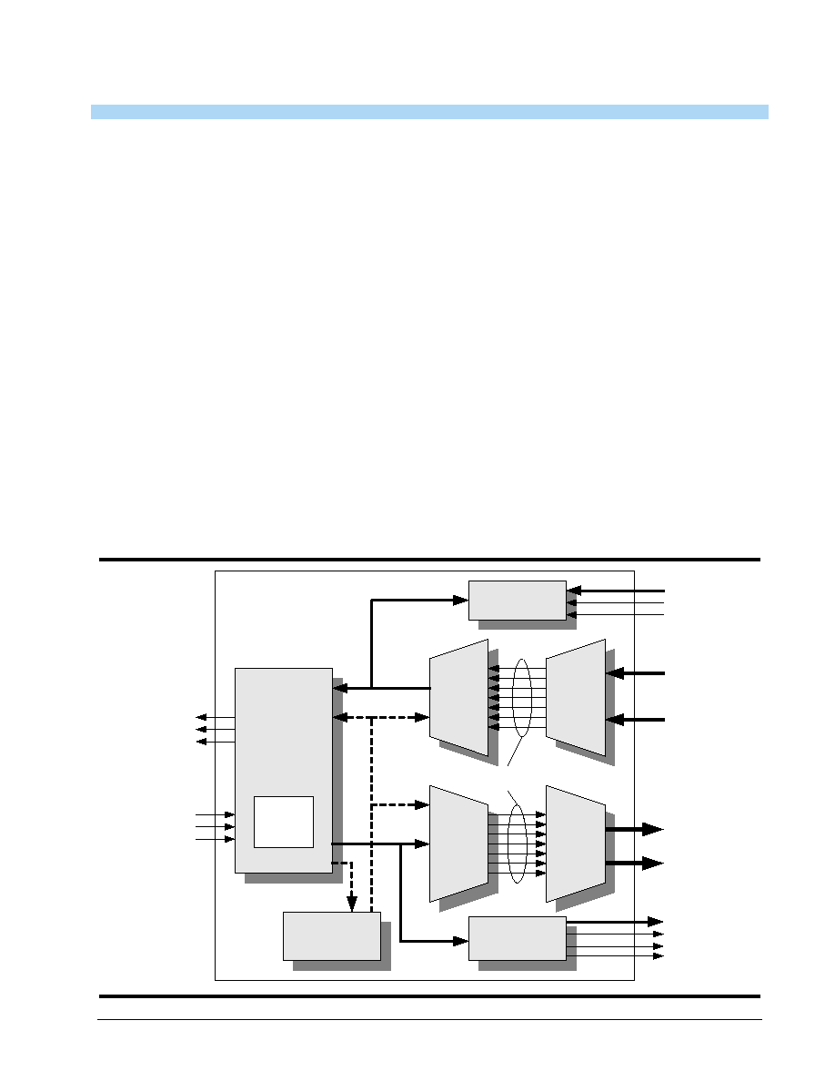
F
IGURE
1. B
LOCK
D
IAGRAM
OF
THE
XRT72L13 M
ULTIPLEXER
/F
RAMER
TxHDLC
Controller
TxHDLC
Controller
RxDS1[0:27]
RxClk[0:27]
M23
DEMUX
M23
DEMUX
M23
MUX
M23
MUX
M12
MUX
M12
MUX
Clear Channel
DS3 Framer
Clear Channel
DS3 Framer
32/64 Bit
De-Jitter
FIFO
RxHDLC
Controller
RxHDLC
Controller
RxHdlc[0:7]
RxHDLCClk
RxIdle
Valid-FCS
TxDS1[0:27]
TxClk[0:27]
TxHDLC[0:7]
TxHDLCClk
Send_FCS
Microprocessor
Interface
Microprocessor
Interface
TxPOS
TxNEG
TxLine Clk
RxPOS
RxNEG
RxLine Clk
DS2 or G.747
Data Streams
M12
DEMUX
XRT72L13
áç
áç
áç
áç
M13 MULTIPLEXER/CLEAR CHANNEL DS3 FRAMER IC
REV. P1.0.6
PRELIMINARY
2
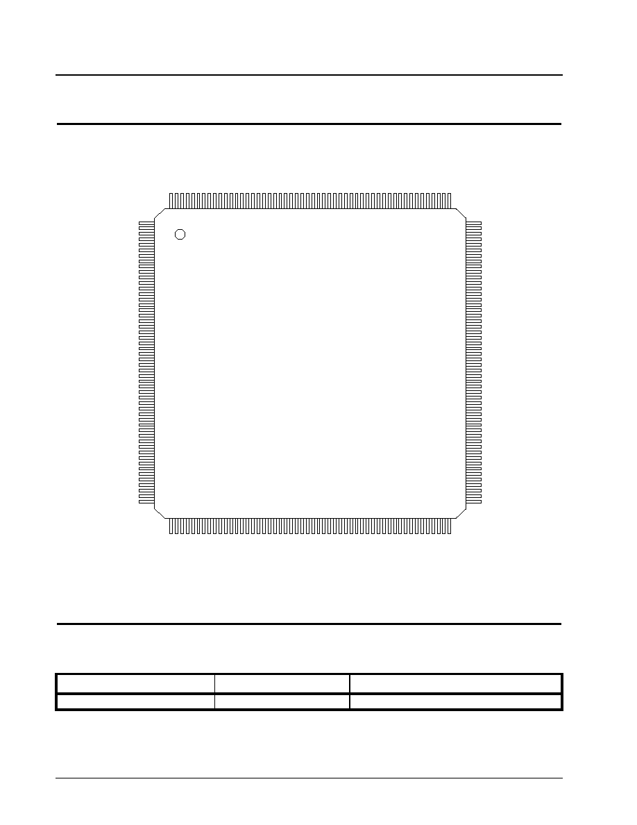
PIN OUT OF THE 72L13 FRAMER IC
RxDS1Data_4/RxHDLC_Data_4
RxDS1Clk_4
RxDS1Data_3/RxHDLC_Data_3
RxDS1Clk_3/RxIDLE
RxDS1Data_2/RxHDLC_Data_2
RxDS1Clk_2/ValidFCS
RxDS1Data_1/RxHDLC_Data_1
RxDS1Clk_1/RxHDLCClk
RxDS1Data_0/RxHDLC_Data_0
VDD
RxDS1Clk_0/TxHDLCClk
RESETB
A0
D0
A1
INTB*
D1
A2
MOTO
GND
D2
A3
Rdy_Dtck
D3
A4
ALE_AS
D4
A5
CSB
D5
A6
RdB_DS
D6
A7
VDD
WRB_RW
D7
A8
GND (TEST MODE)
NIBBLEINTF
TxDS1Data_27/TxHDLCData_7
TxDS1Clk_27/SEND_MSG
TxDS1Data_26/TxHDLCData_6
TxDS1Clk_26/SEND_FCS
TxDS1Data_25/TxHDLCData_5
GND
TxDS1Clk_25
TxDS1Data_24/TxHDLCData_4
TxDS1Clk_24
TxDS1Data_23/TxHDLCData_3
TxDS1Clk_23
TxDS1Data_22/TxHDLCData_2
R x D S 1 D a t a _ 2 6
R x D S 1 C l k _ 2 6
R x D S 1 D a t a _ 2 5
R x D S 1 C l k _ 2 5
R x D S 1 D a t a _ 2 4
R x D S 1 C l k _ 2 4
R x D S 1 D a t a _ 2 3
R x D S 1 C l k _ 2 3
R x D S 1 D a t a _ 2 2
R x D S 1 C l k _ 2 2
V D D
R x D S 1 D a t a _ 2 1
R x D S 1 C l k _ 2 1
R x D S 1 D a t a _ 2 0
R x D S 1 C l k _ 2 0
R x D S 1 D a t a _ 1 9
R x D S 1 C l k _ 1 9
R x D S 1 D a t a _ 1 8
R x D S 1 C l k _ 1 8
R x D S 1 D a t a _ 1 7
R x D S 1 C l k _ 1 7
R x D S 1 D a t a _ 1 6
R x D S 1 C l k _ 1 6
R x D S 1 D a t a _ 1 5
T C K
T M S
T D I
T D O
G N D
R x D S 1 C l k _ 1 5
R x D S 1 D a t a _ 1 4
R x D S 1 C l k _ 1 4
R x D S 1 D a t a _ 1 3
R x D S 1 C l k _ 1 3
R x D S 1 D a t a _ 1 2
R x D S 1 C l k _ 1 2
R x D S 1 D a t a _ 1 1
R x D S 1 C l k _ 1 1
V D D
R x D S 1 D a t a _ 1 0
R x D S 1 C l k _ 1 0
R x D S 1 D a t a _ 9
R x D S 1 C l k _ 9
R x D S 1 D a t a _ 8
R x D S 1 C l k _ 8
R x D S 1 D a t a _ 7 / R x H D L C _ D a t a _ 7
R x D S 1 C l k _ 7
R x D S 1 D a t a _ 6 / R x H D L C _ D a t a _ 6
G N D
R x D S 1 C l k _ 6
R x D S 1 D a t a _ 5 / R x H D L C _ D a t a _ 5
R x D S 1 C l k _ 5
1
2
3
4
5
6
7
8
9
1 0
1 1
1 2
1 3
1 4
1 5
1 6
1 7
1 8
1 9
2 0
2 1
2 2
2 3
2 4
2 5
2 6
2 7
2 8
2 9
3 0
3 1
3 2
3 3
3 4
3 5
3 6
3 7
3 8
3 9
4 0
4 1
4 2
4 3
4 4
4 5
4 6
4 7
4 8
4 9
5 0
5 1
5 2
53
54
55
56
57
58
59
60
61
62
63
64
65
66
67
68
69
70
71
72
73
74
75
76
77
78
79
80
81
82
83
84
85
86
87
88
89
90
91
92
93
94
95
96
97
98
99
100
101
102
103
104
157
158
159
160
161
162
163
164
165
166
167
168
169
170
171
172
173
174
175
176
177
178
179
180
181
182
183
184
185
186
187
188
189
190
191
192
193
194
195
196
197
198
199
200
201
202
203
204
205
206
207
208
1 5 6
1 5 5
1 5 4
1 5 3
1 5 2
1 5 1
1 5 0
1 4 9
1 4 8
1 4 7
1 4 6
1 4 5
1 4 4
1 4 3
1 4 2
1 4 1
1 4 0
1 3 9
1 3 8
1 3 7
1 3 6
1 3 5
1 3 4
1 3 3
1 3 2
1 3 1
1 3 0
1 2 9
1 2 8
1 2 7
1 2 6
1 2 5
1 2 4
1 2 3
1 2 2
1 2 1
1 2 0
1 1 9
1 1 8
1 1 7
1 1 6
1 1 5
1 1 4
1 1 3
1 1 2
1 1 1
1 1 0
1 0 9
1 0 8
1 0 7
1 0 6
1 0 5
2 0 8 L e a d P Q F P
TxFrame
TxInClk
TxNibFrame
TxOHInd/TxPLClkEnb
TxNibClk
TxNib_0/TxSer
TxNib_1
VDD
TxNib_2
TxNib_3
TxOHIns
TxAISEn
TxOHFrame
TxOHEnable
TxOHClk
TxOH
TxNEG
TxPOS
TxLineClk
REQB
TAOS
GND
ENCODIS
TxLEV
RLOOP
LLOOP
DMO
RLOL
ExtLOS
VDD
RxVCOup
RxVCOdown
RxLineClk
RxPOS
RxNEG
RxOH
RxOHEnable
RxOHClk
RxOHFrame
RxLOS
RxNib_3/RxRed
RxNib_2/RxAIS
RxNib_1/RxOOF
GND
RxNib_0/RxSer
RxOutClk
RxOHInd/RxPLClkEnb
RxClk
RxFrame
RxInClk
RxDS1Data_27
RxDS1Clk_27
T x F r a m e R e f
D S 2 O u t C l k
D S 2 I n C l k
T x D S 1 C l k _ 0
T x D S 1 D a t a _ 0
T x D S 1 C l k _ 1
T x D S 1 D a t a _ 1
T x D S 1 C l k _ 2
T x D S 1 D a t a _ 2
T x D S 1 C l k _ 3
G N D
T x D S 1 D a t a _ 3
T x D S 1 C l k _ 4
T x D S 1 D a t a _ 4
T x D S 1 C l k _ 5
T x D S 1 D a t a _ 5
T x D S 1 C l k _ 6
T x D S 1 D a t a _ 6
T x D S 1 C l k _ 7
V D D
T x D S 1 D a t a _ 7
T x D S 1 C l k _ 8
T x D S 1 D a t a _ 8
T x D S 1 C l k _ 9
T x D S 1 D a t a _ 9
T x D S 1 C l k _ 1 0
T x D S 1 D a t a _ 1 0
T x D S 1 C l k _ 1 1
G N D
T x D S 1 D a t a _ 1 1
T x D S 1 C l k _ 1 2
T x D S 1 D a t a _ 1 2
T x D S 1 C l k _ 1 3
T x D S 1 D a t a _ 1 3
T x D S 1 C l k _ 1 4
T x D S 1 D a t a _ 1 4
T x D S 1 C l k _ 1 5
T x D S 1 D a t a _ 1 5
V D D
T x D S 1 C l k _ 1 6
T x D S 1 D a t a _ 1 6
T x D S 1 C l k _ 1 7
T x D S 1 D a t a _ 1 7
T x D S 1 C l k _ 1 8
T x D S 1 D a t a _ 1 8
T x D S 1 C l k _ 1 9
T x D S 1 D a t a _ 1 9
T x D S 1 C l k _ 2 0
T x D S 1 D a t a _ 2 0 / T x H D L C D a t a _ 0
T x D S 1 C l k _ 2 1
T x D S 1 D a t a _ 2 1 / T x H D L C D a t a _ 1
T x D S 1 C l k _ 2 2
ORDERING INFORMATION
P
ART
#
P
ACKAGE
O
PERATING
T
EMPERATURE
XRT72L13IQ
208 pin PQFP
-40°C to +85°C

áç
áç
áç
áç
XRT72L13
M13 MULTIPLEXER/CLEAR CHANNEL DS3 FRAMER IC
PRELIMINARY
REV. P1.0.6
I
TABLE OF CONTENTS
GENERAL DESCRIPTION .................................................................................................. 1
FEATURES ................................................................................................................................................ 1
APPLICATIONS ......................................................................................................................................... 1
Figure 1. Block Diagram of the XRT72L13 Multiplexer/Framer ........................................................... 1
P
IN
OUT
OF
THE
72
L
13
FRAMER
IC
............................................................................................................... 2
ORDERING INFORMATION ...................................................................................................................... 2
ELECTRICAL CHARACTERISTICS ................................................................................. 39
A
BSOLUTE
M
AXIMUMS
................................................................................................................................ 39
DC E
LECTRICAL
C
HARACTERISTICS
............................................................................................................ 39
AC E
LECTRICAL
C
HARACTERISTICS
............................................................................................................ 39
AC E
LECTRICAL
C
HARACTERISTICS
(C
ONT
.) ............................................................................................... 40
Figure 2. Timing Diagram for Transmit Payload Input Interface, when the XRT72L13 is operating in
both the DS3 and Loop-Timing Modes ................................................................................ 43
Figure 3. Timing Diagram for the Transmit Payload Input Interface, when the XRT72L13 is operating
in both the DS3/Serial and Local-Timing Modes ................................................................ 44
Figure 4. Timing Diagram for the Transmit Payload Data Input Interface, when the XRT72L13 is op-
erating in both the DS3/Nibble and Looped-Timing Modes .............................................. 44
Figure 5. Timing Diagram for the Transmit Payload Data Input Interface, when the XRT72L13 is op-
erating in the DS3/Nibble and Local-Timing Modes ........................................................... 45
Figure 6. Timing Diagram for the Transmit Overhead Data Input Interface (Method 1 Access) .... 45
Figure 7. Timing Diagram for the Transmit Overhead Data Input Interface (Method 2 Access) .... 46
Figure 8. Transmit LIU Interface Timing - Framer is configured to update "TxPOS" and "TxNEG" on
the rising edge of "TxLineClk" ............................................................................................. 46
Figure 9. Transmit LIU Interface Timing - Framer is configured to update "TxPOS" and "TxNEG" on
the falling edge of "TxLineClk" ............................................................................................ 47
Figure 10. Receive LIU Interface Timing - Framer is configured to sample "RxPOS" and "RxNEG"
on the rising edge of "RxLineClk" ....................................................................................... 47
Figure 11. Receiver LIU Interface Timing - Framer is configured to sample "RxPOS" and "RxNEG"
on the falling edge of "RxLineClk" ...................................................................................... 48
Figure 12. Receive Payload Data Output Interface Timing (Serial Mode Operation) ...................... 48
Figure 13. Receive Payload Data Output Interface Timing (Nibble Mode Operation) ..................... 49
Figure 14. Receive Overhead Data Output Interface Timing (Method 1 - Using RxOHClk) ............ 49
Figure 15. Receive Overhead Data Output Interface Timing (Method 2 - Using RxOHEnable) ..... 50
Figure 16. Microprocessor Interface Timing - Intel Type Programmed I/O Read Operations ........ 50
Figure 17. Microprocessor Interface Timing - Intel Type Programmed I/O Write Operations ....... 51
Figure 18. Microprocessor Interface Timing - Intel Type Read Burst Access Operation ............... 51
Figure 19. Microprocessor Interface Timing - Intel Type Write Burst Access Operation .............. 52
Figure 20. Microprocessor Interface Timing - Motorola Type Programmed I/O Read Operation .. 52
Figure 21. Microprocessor Interface Timing - Motorola Type Programmed I/O Write Operation .. 53
Figure 22. Microprocessor Interface Timing - Motorola Type Read Burst Access Operation ....... 53
Figure 23. Microprocessor Interface Timing - Motorola Type Write Burst Access Operation ....... 53
Figure 24. Microprocessor Interface Timing - ResetB* Pulse Width ................................................ 53
1.0 SYSTEM DESCRIPTION ................................................................................................................... 54
Figure 25. Block Diagram of the XRT72L13 M13 Multiplexer/Framer IC .......................................... 54
1.1 XRT72L13 OPERATION WHILE IN THE MULTIPLEXER/DE-MULTIPLEXER MODE ................................. 54
Figure 26. Functional Block Diagram of the XRT72L13 M13 Multiplexer/Framer IC, while operating
in the "Multiplexer/De-Multiplexer Mode ............................................................................. 55
1.1.1 In the Transmit Direction ...................................................................................................................... 55
1.1.2 In the Receive Direction ....................................................................................................................... 56
1.1.3 Diagnostic Resources available for MUX/DEMUX Mode ..................................................................... 56
Figure 27. Illustration of the XRT72L13 Operating in the "DS1/E1 Tributary Loop-back Mode ..... 57
Figure 28. Illustration of the XRT72L13 Operating in the "DS2/ITU-T G.747 Tributary Loop-Back

XRT72L13
áç
áç
áç
áç
M13 MULTIPLEXER/CLEAR CHANNEL DS3 FRAMER IC
REV. P1.0.6
PRELIMINARY
II
Mode ....................................................................................................................................... 58
1.2 XRT72L13 OPERATION WHILE IN THE "CLEAR CHANNEL DS3 FRAMER MODE" ................................ 58
Figure 29. Functional Block diagram of the XRT72L13 M13 Multiplexer/Framer IC, while Operating
in the "Clear Channel DS3 Framer Mode" ........................................................................... 59
1.2.1 Operation of the XRT72L13 while in the "Clear Channel DS3 Framer Mode" ..................................... 59
Figure 30. Illustration of the XRT72L13 M13 Multiplexer/Framer operating in the "Clear Channel DS3
Framer Local Loop-back" Mode ........................................................................................... 60
Figure 31. Illustration of the XRT72L13 M13 Multiplexer/Framer operating in the "Clear Channel DS3
Framer Remote Loop-back" Mode ....................................................................................... 61
1.3 XRT72L13 OPERATION WHILE IN THE "HIGH SPEED HDLC CONTROLLER" MODE ............................. 61
Figure 32. Illustration of the XRT72L13 M13 Multiplexer/Framer IC, when it has been configured to
operate in the "High Speed HDLC Controller" Mode ......................................................... 62
2.0 The Microprocessor Interface Block .............................................................................................. 62
Figure 33. Simple Block Diagram of the Microprocessor Interface Block, within the Framer IC .. 63
2.1 T
HE
M
ICROPROCESSOR
I
NTERFACE
B
LOCK
S
IGNAL
........................................................................................... 63
T
ABLE
1: D
ESCRIPTION
OF
THE
M
ICROPROCESSOR
I
NTERFACE
S
IGNALS
THAT
EXHIBIT
CONSTANT
ROLES
IN
BOTH
THE
"I
NTEL
"
AND
"M
OTOROLA
" M
ODES
...................................................................................... 64
T
ABLE
2: P
IN
D
ESCRIPTION
OF
M
ICROPROCESSOR
I
NTERFACE
S
IGNALS
- W
HILE
THE
M
ICROPROCESSOR
I
NTER
-
FACE
IS
O
PERATING
IN
THE
I
NTEL
M
ODE
..................................................................................... 64
T
ABLE
3: P
IN
D
ESCRIPTION
OF
THE
M
ICROPROCESSOR
I
NTERFACE
S
IGNALS
WHILE
THE
M
ICROPROCESSOR
I
N
-
TERFACE
IS
OPERATING
IN
THE
M
OTOROLA
M
ODE
...................................................................... 65
2.2 I
NTERFACING
THE
XRT 72L13 DS3 F
RAMER
TO
THE
L
OCAL
µC/µP
OVER
VIA
THE
M
ICROPROCESSOR
I
NTERFACE
B
LOCK
65
2.2.1 Interfacing the XRT 72L13 DS3 Framer to the Microprocessor over an 8 bit wide bi-directional Data Bus
65
2.2.2 Data Access Modes ............................................................................................................................. 66
Figure 34. Behavior of Microprocessor Interface signals during an "Intel-type" Programmed I/O
Read Operation ...................................................................................................................... 67
Figure 35. Behavior of the Microprocessor Interface Signals, during an "Intel-type" Programmed I/
O Write Operation .................................................................................................................. 68
Figure 36. Illustration of the Behavior of Microprocessor Interface signals, during a "Motorola-type"
Programmed I/O Read Operation ......................................................................................... 69
Figure 37. Illustration of the Behavior of the Microprocessor Interface signal, during a "Motorola-
type" Programmed I/O Write Operation ............................................................................... 70
Figure 38. Behavior of the Microprocessor Interface Signals, during the "Initial" Read Operation of
a Burst Cycle (Intel Type Processor) ................................................................................... 72
Figure 39. Behavior of the Microprocessor Interface Signals, during subsequent "Read" Operations
within the Burst I/O Cycle ..................................................................................................... 73
Figure 40. Behavior of the Microprocessor Interface signals, during the "Initial" Write Operation of
a Burst Cycle (Intel-type Processor) .................................................................................... 74
Figure 41. Behavior of the Microprocessor Interface Signals, during subsequent "Write" Operations
within the Burst I/O Cycle ..................................................................................................... 75
Figure 42. Behavior of the Microprocessor Interface Signals, during the "Initial" Read Operation of
a Burst Cycle (Motorola Type Processor) ........................................................................... 76
Figure 43. Behavior the Microprocessor Interface Signals, during subsequent "Read" Operations
within the Burst I/O Cycle (Motorola-type µC/µP) ............................................................... 77
Figure 44. Behavior of the Microprocessor Interface signals, during the "Initial" Write Operation of
a Burst Cycle (Motorola-type Processor) ............................................................................ 78
Figure 45. Behavior of the Microprocessor Interface Signals, during subsequent "Write" Operations
with the Burst I/O Cycle (Motorola-type µC/µP) .................................................................. 79
2.3 O
N
-C
HIP
R
EGISTER
O
RGANIZATION
.................................................................................................................. 79
2.3.1 Framer Register Addressing ................................................................................................................ 79
2.3.2 M13 Mux/Framer Register Description ................................................................................................. 79
T
ABLE
4: R
EGISTER
A
DDRESS
M
AP
........................................................................................................... 80
O
PERATING
M
ODE
R
EGISTER
(A
DDRESS
= 0
X
00) ........................................................................................ 83

áç
áç
áç
áç
XRT72L13
M13 MULTIPLEXER/CLEAR CHANNEL DS3 FRAMER IC
PRELIMINARY
REV. P1.0.6
III
I/O C
ONTROL
R
EGISTER
(A
DDRESS
= 0
X
01) ............................................................................................... 84
P
ART
N
UMBER
R
EGISTER
(A
DDRESS
= 0
X
02) ............................................................................................. 85
V
ERSION
N
UMBER
R
EGISTER
(A
DDRESS
= 0
X
03) ........................................................................................ 85
B
LOCK
I
NTERRUPT
ENABLE
R
EGISTER
(A
DDRESS
= 0
X
04) .......................................................................... 86
B
LOCK
I
NTERRUPT
S
TATUS
R
EGISTER
(A
DDRESS
= 0
X
05) ......................................................................... 86
RX
F
IFO
CONTROL
R
EGISTER
(A
DDRESS
= 0
X
06) ........................................................................................ 87
M23 C
ONFIGURATION
R
EGISTER
(A
DDRESS
= 0
X
07) ................................................................................. 87
T
ABLE
5: ................................................................................................................................................. 89
M23 T
X
DS2 AIS R
EGISTER
(A
DDRESS
= 0
X
08) ....................................................................................... 89
M23
REQUEST
LOOPBACK
R
EGISTER
(A
DDRESS
= 0
X
09) ........................................................................... 90
M23 L
OOPBACK
ACTIVATION
R
EGISTER
(A
DDRESS
= 0
X
0A) ....................................................................... 90
M23 R
X
DS2 AIS R
EGISTER
(A
DDRESS
= 0
X
0B) ...................................................................................... 90
DS3 T
EST
R
EGISTER
(A
DDRESS
= 0
X
0C) .................................................................................................. 91
RX
DS
3
CONFIGURATION
AND
STATUS
R
EGISTER
(A
DDRESS
= 0
X
10) ........................................................... 92
RX
DS
3
STATUS
R
EGISTER
(A
DDRESS
= 0
X
11) ........................................................................................... 93
RX
DS
3
INTERRUPT
ENABLE
R
EGISTER
(A
DDRESS
= 0
X
12) ......................................................................... 94
R
X
D
S
3 I
NTERRUPT
S
TATUS
R
EGISTER
(A
DDRESS
= 0
X
13) ........................................................................ 95
R
X
D
S
3
SYNC
DETECT
R
EGISTER
(A
DDRESS
= 0
X
14) ................................................................................. 96
R
X
DS3 FEAC I
NTERRUPT
E
NABLE
/S
TATUS
R
EGISTER
(A
DDRESS
= 0
X
17) .................................................. 97
R
X
DS3 LAPD C
ONTROL
R
EGISTER
(A
DDRESS
= 0
X
18) .............................................................................. 97
R
X
DS3 LAPD S
TATUS
R
EGISTER
(A
DDRESS
= 0
X
19) ................................................................................ 98
M12 DS2 # 1 C
ONFIGURATION
R
EGISTER
(A
DDRESS
= 0
X
1A) .................................................................... 99
M12 DS2 # 2 C
ONFIGURATION
R
EGISTER
(A
DDRESS
= 0
X
1B) .................................................................. 100
M12 DS2 # 3 C
ONFIGURATION
R
EGISTER
(A
DDRESS
= 0
X
1C) .................................................................. 100
M12 DS2 # 4 C
ONFIGURATION
R
EGISTER
(A
DDRESS
= 0
X
1D) .................................................................. 101
M12 DS2 # 5 C
ONFIGURATION
R
EGISTER
(A
DDRESS
= 0
X
1E) .................................................................. 102
M12 DS2 # 6 C
ONFIGURATION
R
EGISTER
(A
DDRESS
= 0
X
1F) .................................................................. 103
M12 DS2 # 7 C
ONFIGURATION
R
EGISTER
(A
DDRESS
= 0
X
20) .................................................................. 104
M12 DS2 # 1 A
IS
R
EGISTER
(A
DDRESS
= 0
X
21) ...................................................................................... 105
M12 DS2 # 2 A
IS
R
EGISTER
(A
DDRESS
= 0
X
22) ...................................................................................... 106
M12 DS2 # 3 A
IS
R
EGISTER
(A
DDRESS
= 0
X
23) ...................................................................................... 107
M12 DS2 # 4 A
IS
R
EGISTER
(A
DDRESS
= 0
X
24) ...................................................................................... 108
M12 DS2 # 5 A
IS
R
EGISTER
(A
DDRESS
= 0
X
25) ...................................................................................... 109
M12 DS2 # 6 A
IS
R
EGISTER
(A
DDRESS
= 0
X
26) ...................................................................................... 110
M12 DS2 # 7 A
IS
R
EGISTER
(A
DDRESS
= 0
X
27) ...................................................................................... 111
M12 DS2 # 1 L
OOP
-
BACK
R
EGISTER
(A
DDRESS
= 0
X
28) ......................................................................... 112
M12 DS2 # 2 L
OOP
-
BACK
R
EGISTER
(A
DDRESS
= 0
X
29) ......................................................................... 113
M12 DS2 # 3 L
OOP
-
BACK
R
EGISTER
(A
DDRESS
= 0
X
2A) ........................................................................ 114
M12 DS2 # 4 L
OOP
-
BACK
R
EGISTER
(A
DDRESS
= 0
X
2B) ........................................................................ 116
M12 DS2 # 5 L
OOP
-
BACK
R
EGISTER
(A
DDRESS
= 0
X
2C) ........................................................................ 117
M12 DS2 # 6 L
OOP
-
BACK
R
EGISTER
(A
DDRESS
= 0
X
2D) ........................................................................ 118
M12 DS2 # 7 L
OOP
-
BACK
R
EGISTER
(A
DDRESS
= 0
X
28) ......................................................................... 119
T
X
DS3 C
ONFIGURATION
R
EGISTER
(A
DDRESS
= 0
X
30) ........................................................................... 120
T
RANSMIT
DS3 C
ONFIGURATION
& S
TATUS
R
EGISTER
(A
DDRESS
= 0
X
31) ................................................ 121
T
X
DS3 FEAC R
EGISER
(A
DDRESS
= 0
X
32) ............................................................................................ 122
T
X
DS3 LAPD C
ONFIGURATION
R
EGISTER
(A
DDRESS
= 0
X
33) .................................................................. 122
T
X
DS3 LAPD S
TATUS
AND
I
NTERRUPT
R
EGISTER
(A
DDRESS
= 0
X
34) ...................................................... 123
T
X
DS3 M-B
IT
M
ASK
R
EGISTER
(A
DDRESS
= 0
X
35) .................................................................................. 124
T
X
DS3 F-B
IT
M
ASK
R
EGISTER
- 1 (A
DDRESS
= 0
X
36) ............................................................................. 124
T
X
DS3 F-B
IT
M
ASK
R
EGISTER
- 2 (A
DDRESS
= 0
X
37) .............................................................................. 125
T
X
DS3 F-B
IT
M
ASK
R
EGISTER
- 3 (A
DDRESS
= 0
X
38) ............................................................................. 125
T
X
DS3 F-B
IT
M
ASK
R
EGISTER
- 4 (A
DDRESS
= 0
X
39) .............................................................................. 125
DS2 # 1 F
RAMER
C
ONFIGURATION
REGISTER
(A
DDRESS
= 0
X
3A) ............................................................ 126
DS2 # 2 F
RAMER
C
ONFIGURATION
REGISTER
(A
DDRESS
= 0
X
3B) ............................................................ 127
Document Outline
- Main Menu
- Products
- XRT72L13 Menu
- Alphanumeric Index
- Search