 | –≠–ª–µ–∫—Ç—Ä–æ–Ω–Ω—ã–π –∫–æ–º–ø–æ–Ω–µ–Ω—Ç: EIC0910-4 | –°–∫–∞—á–∞—Ç—å:  PDF PDF  ZIP ZIP |
EIC0910-4
Specifications are subject to change without notice.
Excelics Semiconductor, Inc. 310 De Guigne Drive, Sunnyvale, CA 94085
page 1 of 4
Phone: 408-737-1711 Fax: 408-737-1868 Web:
www.excelics.com
Revised April 2004
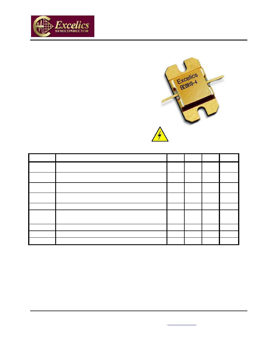
9.50-10.50 GHz 4-Watt Internally-Matched Power FET
Issued Date: 04-27-04
FEATURES
∑
9.50-10.50
GHz
Bandwidth
∑
Input/Output Impedance Matched to 50 Ohms
∑
+36.5 dBm Output Power at 1dB Compression
∑
7.5 dB Power Gain at 1dB Compression
∑
30% Power Added Efficiency
∑
-46 dBc IM3 at Po = 25.5 dBm SCL
∑
Hermetic Metal Flange Package
∑
100% Tested for DC, RF, and R
TH
DESCRIPTION
The EIC0910-4 is a high power, highly linear,
single stage MFET amplifier in a flange mount
package. This amplifier features Excelics' unique
PHEMT transistor technology.
Caution! ESD sensitive device.
ELECTRICAL CHARACTERISTICS (T
a
= 25
∞
C)
SYMBOL PARAMETERS/TEST
CONDITIONS
1
MIN
TYP
MAX
UNITS
P
1dB
Output Power at 1dB Compression f = 9.50-10.50GHz
V
DS
= 10 V, I
DSQ
= 1100mA
35.5 36.5
dBm
G
1dB
Gain at 1dB Compression f = 9.50-10.50GHz
V
DS
= 10 V, I
DSQ
= 1100mA
6.5 7.5 dB
G
Gain Flatness f = 9.50-10.50GHz
V
DS
= 10 V, I
DSQ
= 1100mA
±0.6
dB
PAE
Power Added Efficiency at 1dB Compression
V
DS
= 10 V, I
DSQ
= 1100mA f = 9.50-10.50GHz
30 %
Id
1dB
Drain Current at 1dB Compression f = 9.50-10.50GHz
1200
1300
mA
IM3
Output 3rd Order Intermodulation Distortion
f = 10 MHz 2-Tone Test; Pout = 25.5 dBm S.C.L
2
V
DS
= 10 V, I
DSQ
65% IDSS
f = 10.50GHz
-43 -46
dBc
I
DSS
Saturated Drain Current
V
DS
= 3 V, V
GS
= 0 V
2000
2500
mA
V
P
Pinch-off Voltage
V
DS
= 3 V, I
DS
= 20 mA
-2.5
-4.0
V
R
TH
Thermal Resistance
3
5.5
6.0
o
C/W
Notes:
1.
Tested with 100 Ohm gate resistor.
2.
S.C.L. = Single Carrier Level.
3.
Overall Rth depends on case mounting.
EIC0910-4
Specifications are subject to change without notice.
Excelics Semiconductor, Inc. 310 De Guigne Drive, Sunnyvale, CA 94085
page 2 of 4
Phone: 408-737-1711 Fax: 408-737-1868 Web:
www.excelics.com
Revised April 2004
Issued Date: 04-27-04
ABSOLUTE MAXIMUM RATINGS FOR CONTINUOUS OPERATION
1,2
SYMBOL CHARACTERISTIC
VALUE
V
DS
Drain to Source Voltage
10 V
V
GS
Gate to Source Voltage
-4.5 V
I
DS
Drain
Current
IDSS
I
GSF
Forward Gate Current
40 mA
P
IN
Input Power
@ 3dB compression
P
T
Total Power Dissipation
20 W
T
CH
Channel
Temperature
150∞C
T
STG
Storage
Temperature
-65/+150∞C
Notes:
1.
Operating the device beyond any of the above ratings may result in permanent damage or reduction of MTTF.
2.
Bias conditions must also satisfy the following equation P
T
< (T
CH
≠T
PKG
)/R
TH
; where T
PKG
= temperature of package, and
P
T
= (V
DS
* I
DS
) ≠ (P
OUT
≠ P
IN
).
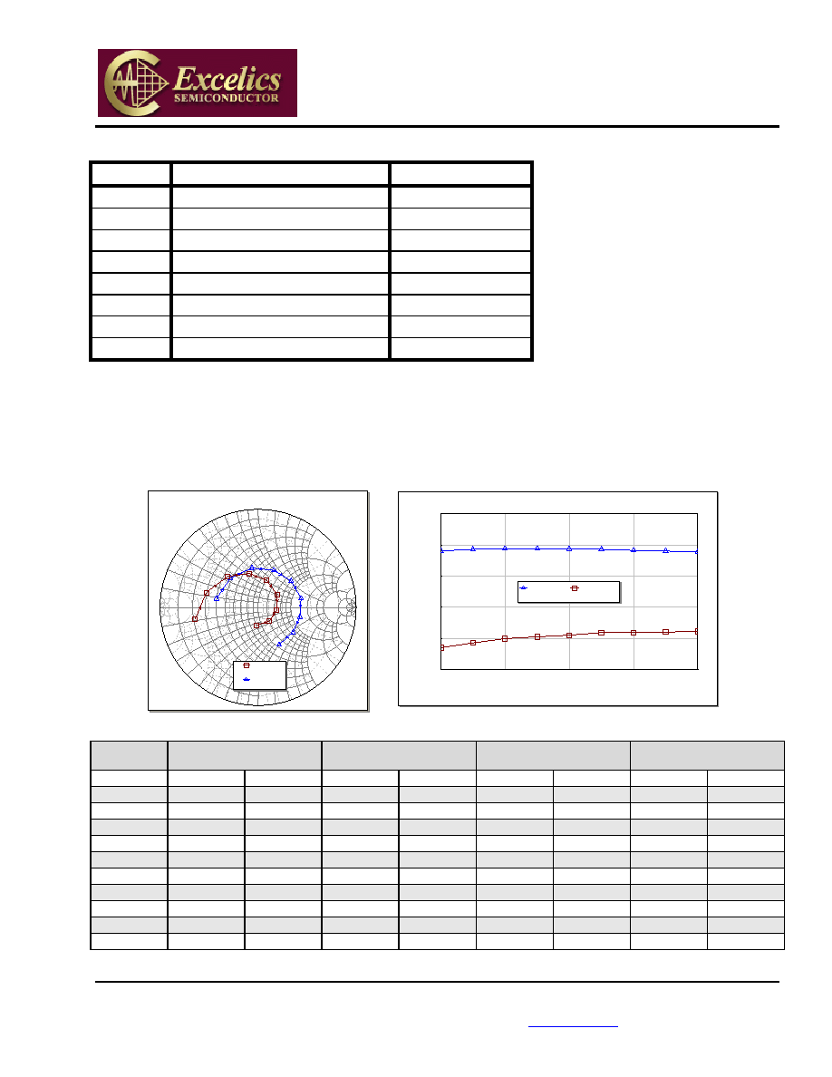
PERFORMANCE DATA
Typical S-Parameters (T= 25∞C, 50
system, de-embedded to edge of package)
V
DS
= 10 V, I
DSQ
= 1100mA
0
1.
0
-1
.0
1.
0
1
0.0
-10.0
10.
0
5.
0
-5.0
5.0
2.
0
-2
.0
2.
0
3.
0
-3.
0
3.0
4.
0
-4.0
4.0
0.
2
-0.
2
0.2
0.
4
-0
.4
0.
4
0.
6
-0
.6
0.
6
0.
8
-
0
.
8
0
.
8
0
1.
0
1.
0
-1.
0
10
.0
10.0
-1
0.
0
5.
0
5.0
-5
.0
2.
0
2.
0
-2
.0
3.
0
3.
0
-3
.0
4.
0
4.
0
-4
.0
0.
2
0.2
-0.
2
0.
4
0.
4
-0
.4
0.
6
0.
6
-0
.6
0.
8
0
.
8
-
0
.
8
S11 and S22
Swp Max
11GHz
Swp Min
9GHz
S[1,1] *
EIC0910-4
S[2,2] *
EIC0910-4
9
9.5
10
10.5
11
Frequency (GHz)
S21 and S12
-30
-20
-10
0
10
20
S2
1
an
d S
1
2 (d
B
)
DB(|S[2,1]|) *
EIC0910-4
DB(|S[1,2]|) *
EIC0910-4
FREQ
--- S11 ---
--- S21 ---
--- S12 ---
--- S22 ---
(GHz)
MAG
ANG
MAG
ANG
MAG
ANG
MAG
ANG
8.75 0.737
-144.630
2.269 -6.970 0.057 -49.810 0.470 -160.060
9.00
0.655
-169.280
2.531
-33.010
0.071
-78.500
0.435
168.080
9.25 0.549
164.010
2.683
-59.860 0.085 -105.960 0.411 133.320
9.50
0.444
134.710
2.765
-86.790
0.100
-134.450
0.408
99.190
9.75 0.357
104.470
2.755
-112.980 0.106 -161.110 0.411 66.750
10.00
0.289
72.550
2.727
-137.970
0.113
174.650
0.431
38.790
10.25 0.235 33.570 2.687
-163.320 0.124 150.320 0.447 11.850
10.50
0.191
-9.260
2.581
172.160
0.124
124.660
0.437
-12.860
10.75 0.179 -51.300 2.519 148.030 0.127 101.940 0.436 -35.330
11.00
0.182
-94.880
2.427
123.370
0.129
78.470
0.436
-60.600
11.25 0.183
-136.850
2.332 98.400 0.131 53.300 0.431 -86.500
EIC0910-4
Specifications are subject to change without notice.
Excelics Semiconductor, Inc. 310 De Guigne Drive, Sunnyvale, CA 94085
page 3 of 4
Phone: 408-737-1711 Fax: 408-737-1868 Web:
www.excelics.com
Revised April 2004
Issued Date: 04-27-04
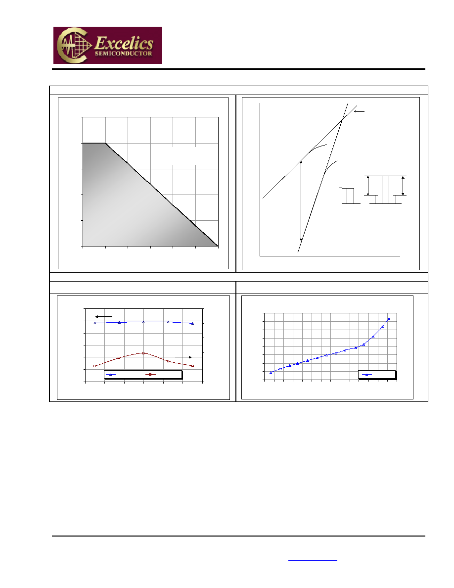
Power De-rating Curve and IM3 Definition
Power Dissipation vs. Temperature
0
5
10
15
20
25
0
25
50
75
100
125
150
Case Temperature (∞C)
T
o
tal
P
o
w
e
r
D
i
s
s
i
pat
i
on (
W
)
Safe Operating
Region
Potentially Unsafe
Operating Region
f1 f2
(2f1-f2) f1 f2 (2f2-f1)
IM3
Pout
Pin
IP
3
= Pout + IM3/2
THIRD-ORDER
INTERCEPT POINT IP3
f1 or f2
(2f2 - f1) or (2f1 - f2)
Pin [S.C.L.] (dBm)
P
o
u
t
[S
.C.L
.]
(
d
B
m
)
IM3
Typical Power Data (V
DS
= 10 V, I
DSQ
= 1100 mA)
Typical IM3 Data (V
DS
= 10 V,
I
DSQ
65% IDSS
)
P-1dB & G-1dB vs Frequency
32.00
33.00
34.00
35.00
36.00
37.00
38.00
9.4
9.6
9.8
10.0
10.2
10.4
10.6
Frequency (GHz)
P
-
1
d
B (d
Bm
)
6.00
7.00
8.00
9.00
10.00
11.00
G
-
1dB
(
d
B
)
P-1dB (dBm)
G-1dB (dB)
IM3 vs Output Power
f1 = 9.50 GHz, f2 = 9.51 GHz
-65
-60
-55
-50
-45
-40
-35
-30
-25
17 18 19 20 21 22 23 24 25 26 27 28 29 30 31
Pout [S.C.L.] (dBm)
IM
3 (
d
B
c
)
IM3 (dBc)
EIC0910-4
Specifications are subject to change without notice.
Excelics Semiconductor, Inc. 310 De Guigne Drive, Sunnyvale, CA 94085
page 4 of 4
Phone: 408-737-1711 Fax: 408-737-1868 Web:
www.excelics.com
Revised April 2004
Issued Date: 04-27-04
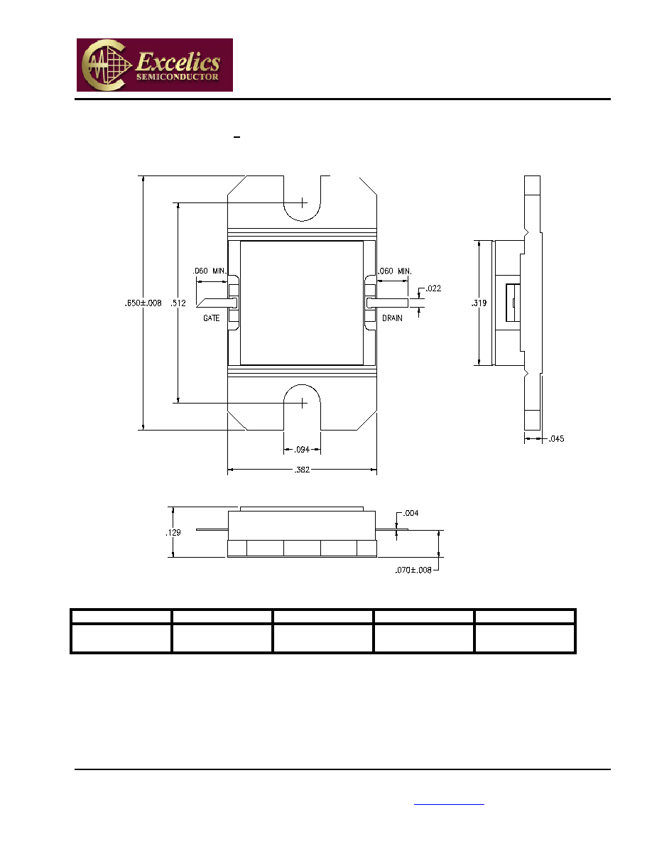
PACKAGE OUTLINE
Dimensions in inches, Tolerance + .005 unless otherwise specified
Excelics
SN
YM
ORDERING INFORMATION
Part Number
Grade
1
f
Test
(GHz)
P
1dB
(min)
IM
3
(min)
2
EIC0910-4 Industrial
9.50-10.50
GHz 35.5
-43.0
Notes: 1. Contact factory for military and hi-rel grades.
2. Exact test conditions are specified in "Electrical Characteristics" table.
EIC0910-4
SOURCE