 | –≠–ª–µ–∫—Ç—Ä–æ–Ω–Ω—ã–π –∫–æ–º–ø–æ–Ω–µ–Ω—Ç: EIC1213-4 | –°–∫–∞—á–∞—Ç—å:  PDF PDF  ZIP ZIP |
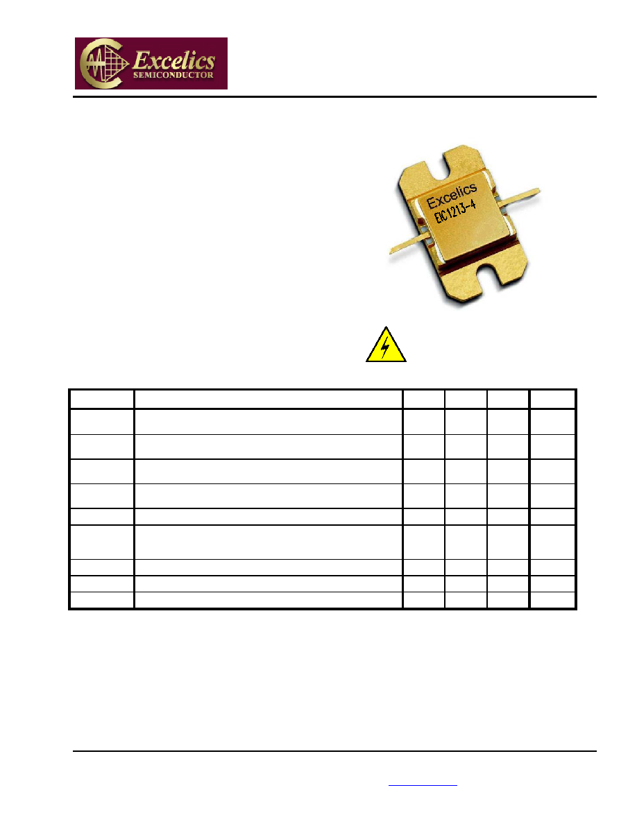
EIC1213-4
Specifications are subject to change without notice.
Excelics Semiconductor, Inc. 310 De Guigne Drive, Sunnyvale, CA 94085
page 1 of 4
Phone: 408-737-1711 Fax: 408-737-1868 Web:
www.excelics.com
Revised October 2003
12.7-13.2 GHz 4-Watt Internally-Matched Power FET
FEATURES
∑
12.7-13.2 GHz Bandwidth
∑
Input/Output Impedance Matched to 50 Ohms
∑
+36.0 dBm Output Power at 1dB Compression
∑
6.5 dB Power Gain at 1dB Compression
∑
28% Power Added Efficiency
∑
-44 dBc IM3 at Po = 25.5 dBm SCL
∑
Hermetic Metal Flange Package
∑
100% Tested for DC, RF, and R
TH
DESCRIPTION
The EIC1213-4 is a high power, highly linear,
single stage MFET amplifier in a flange mount
package. This amplifier features Excelics' unique
MESFET transistor technology.
Caution! ESD sensitive device.
ELECTRICAL CHARACTERISTICS (T
a
= 25
∞
C)
SYMBOL PARAMETERS/TEST
CONDITIONS
1
MIN
TYP
MAX
UNITS
P
1dB
Output Power at 1dB Compression f = 12.7-13.2GHz
V
DS
= 10 V, I
DSQ
1100mA
35.5 36.0
dBm
G
1dB
Gain at 1dB Compression f = 12.7-13.2GHz
V
DS
= 10 V, I
DSQ
1100mA
5.5 6.5 dB
G
Gain Flatness f = 12.7-13.2GHz
V
DS
= 10 V, I
DSQ
1100mA
±0.6
dB
PAE
Power Added Efficiency at 1dB Compression
V
DS
= 10 V, I
DSQ
1100mA f = 12.7-13.2GHz
28 %
Id
1dB
Drain Current at 1dB Compression f = 12.7-13.2GHz
1100
1300
mA
IM3
Output 3rd Order Intermodulation Distortion
f = 10 MHz 2-Tone Test; Pout = 25.5 dBm S.C.L
2
V
DS
= 10 V, I
DSQ
65% IDSS
f = 13.2GHz
-42 -44 dBc
I
DSS
Saturated Drain Current
V
DS
= 3 V, V
GS
= 0 V
1280
2080
2880
mA
V
P
Pinch-off Voltage
V
DS
= 3 V, I
DS
= 20 mA
-2.5
-4.0
V
R
TH
Thermal Resistance
3
5.5
6.0
o
C/W
Notes:
1.
Tested with 100 Ohm gate resistor.
2.
S.C.L. = Single Carrier Level.
3.
Overall Rth depends on case mounting.
EIC1213-4
Specifications are subject to change without notice.
Excelics Semiconductor, Inc. 310 De Guigne Drive, Sunnyvale, CA 94085
page 2 of 4
Phone: 408-737-1711 Fax: 408-737-1868 Web:
www.excelics.com
Revised October 2003
ABSOLUTE MAXIMUM RATINGS FOR CONTINUOUS OPERATION
1,2
SYMBOL CHARACTERISTIC
VALUE
V
DS
Drain to Source Voltage
10 V
V
GS
Gate to Source Voltage
-4.5 V
I
DS
Drain
Current
IDSS
I
GSF
Forward Gate Current
40 mA
P
IN
Input Power
@ 3dB compression
P
T
Total Power Dissipation
21 W
T
CH
Channel
Temperature
150∞C
T
STG
Storage
Temperature
-65/+150∞C
Notes:
1.
Operating the device beyond any of the above ratings may result in permanent damage or reduction of MTTF.
2.
Bias conditions must also satisfy the following equation P
T
< (T
CH
≠T
PKG
)/R
TH
; where T
PKG
= temperature of package, and
P
T
= (V
DS
* I
DS
) ≠ (P
OUT
≠ P
IN
).
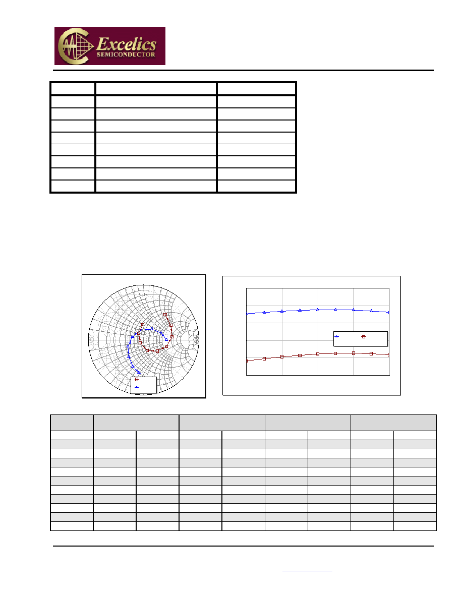
PERFORMANCE DATA
Typical S-Parameters (T= 25∞C, 50
system, de-embedded to edge of package)
V
DS
= 10 V, I
DSQ
1100mA
0
1.
0
-1.
0
1.0
1
0.0
-10.0
10.
0
5.
0
-5.0
5.0
2.
0
-2
.0
2.
0
3.
0
-3.
0
3.0
4.
0
-4.
0
4.0
0.
2
-0.
2
0.2
0.
4
-0
.4
0.
4
0.
6
-0
.6
0.
6
0.
8
-
0
.
8
0
.
8
0
1.0
1.
0
-
1.0
10.
0
10.0
-1
0.
0
5.0
5.0
-5.
0
2.0
2.
0
-2
.0
3.0
3.
0
-3
.0
4.0
4.
0
-4
.0
0.2
0.2
-0.
2
0.4
0.
4
-0
.4
0.6
0.
6
-0
.6
0.8
0
.
8
-
0
.
8
S11 and S22
Swp Max
14GHz
Swp Min
12GHz
S[1,1] *
EIC1213-4
S[2,2] *
EIC1213-4
12
12.5
13
13.5
14
Frequency (GHz)
S21 and S12
-30
-20
-10
0
10
20
S2
1
an
d S
1
2 (d
B
)
DB(|S[2,1]|) *
EIC1213-4
DB(|S[1,2]|) *
EIC1213-4
FREQ
--- S11 ---
--- S21 ---
--- S12 ---
--- S22 ---
(GHz)
MAG
ANG
MAG
ANG
MAG
ANG
MAG
ANG
12.0 0.6013 49.54 1.8523 -73.04 0.0813 -101.01 0.602 -98.17
12.2
0.5629
32.76
1.9838
-88.24
0.0911
-116.63
0.5402
-109.62
12.4 0.5404 14.98 2.1132
-104.28
0.1011 -132.11 0.4471 -123.24
12.6
0.4871
-2.5
2.234
-121.18
0.1114
-148.78
0.3645
-140.48
12.8 0.4055 -19.9 2.3293 -138.38 0.1196 -166.24 0.2874 -163.34
13.0
0.3196
-39.9
2.4047
-156.51
0.1284
176.28
0.2125
163.54
13.2 0.2249 -63.97 2.4359
-175.14 0.1342 158.11 0.179 117.02
13.4
0.118
-101.47
2.4042
166.07
0.1355
139.57
0.2111
71.43
13.6 0.0879 170.88 2.322 147.76 0.1342 121.8 0.2843 38.35
13.8
0.1766
117.33
2.1849
129.28
0.1288
104.29
0.3574
16.48
14.0 0.2745 92.92 2.0299 112.36 0.1226 87.32 0.4104 0.75
EIC1213-4
Specifications are subject to change without notice.
Excelics Semiconductor, Inc. 310 De Guigne Drive, Sunnyvale, CA 94085
page 3 of 4
Phone: 408-737-1711 Fax: 408-737-1868 Web:
www.excelics.com
Revised October 2003
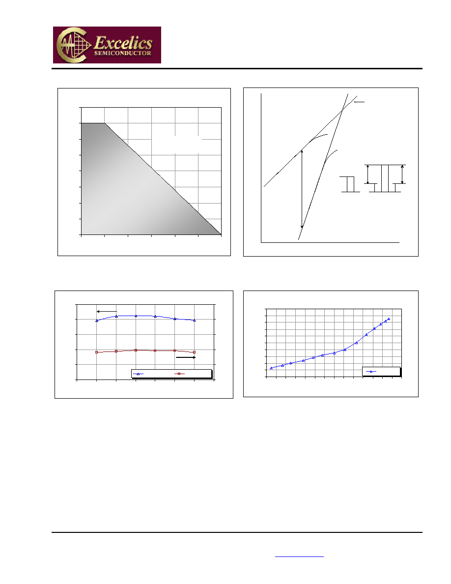
Power De-rating Curve and IM3 Definition
Power Dissipation vs. Temperature
0
3
6
9
12
15
18
21
24
0
25
50
75
100
125
150
Case Temperature (∞C)
T
o
t
a
l P
o
w
e
r
D
i
s
s
ip
a
t
io
n
(
W
)
Safe Operating
Region
Potentially Unsafe
Operating Region
f1 f2
(2f1-f2) f1 f2 (2f2-f1)
IM3
Pout
Pin
IP
3
= Pout + IM3/2
THIRD-ORDER
INTERCEPT POINT IP3
f1 or f2
(2f2 - f1) or (2f1 - f2)
Pin [S.C.L.] (dBm)
P
o
u
t
[S
.C
.L
.
]
(
d
B
m
)
IM3
Typical Power Data (V
DS
= 10 V, I
DSQ
= 1100 mA)
Typical IM3 Data (V
DS
= 10 V,
I
DSQ
65% IDSS
)
P-1dB & G-1dB vs Frequency
33
34
35
36
37
38
12.6
12.7
12.8
12.9
13.0
13.1
13.2
13.3
Frequency (GHz)
P-1
d
B (d
Bm
)
4
5
6
7
8
9
G
-
1dB
(
d
B
)
P-1dB (dBm)
G-1dB (dB)
IM3 vs Output Power
f1 = 13.20 GHz, f2 = 13.21 GHz
-65
-60
-55
-50
-45
-40
-35
-30
-25
-20
-15
19 20 21 22 23 24 25 26 27 28 29 30 31 32 33
Pout [S.C.L.] (dBm)
IM
3
(d
B
c
)
IM3 (dBc)
EIC1213-4
Specifications are subject to change without notice.
Excelics Semiconductor, Inc. 310 De Guigne Drive, Sunnyvale, CA 94085
page 4 of 4
Phone: 408-737-1711 Fax: 408-737-1868 Web:
www.excelics.com
Revised October 2003
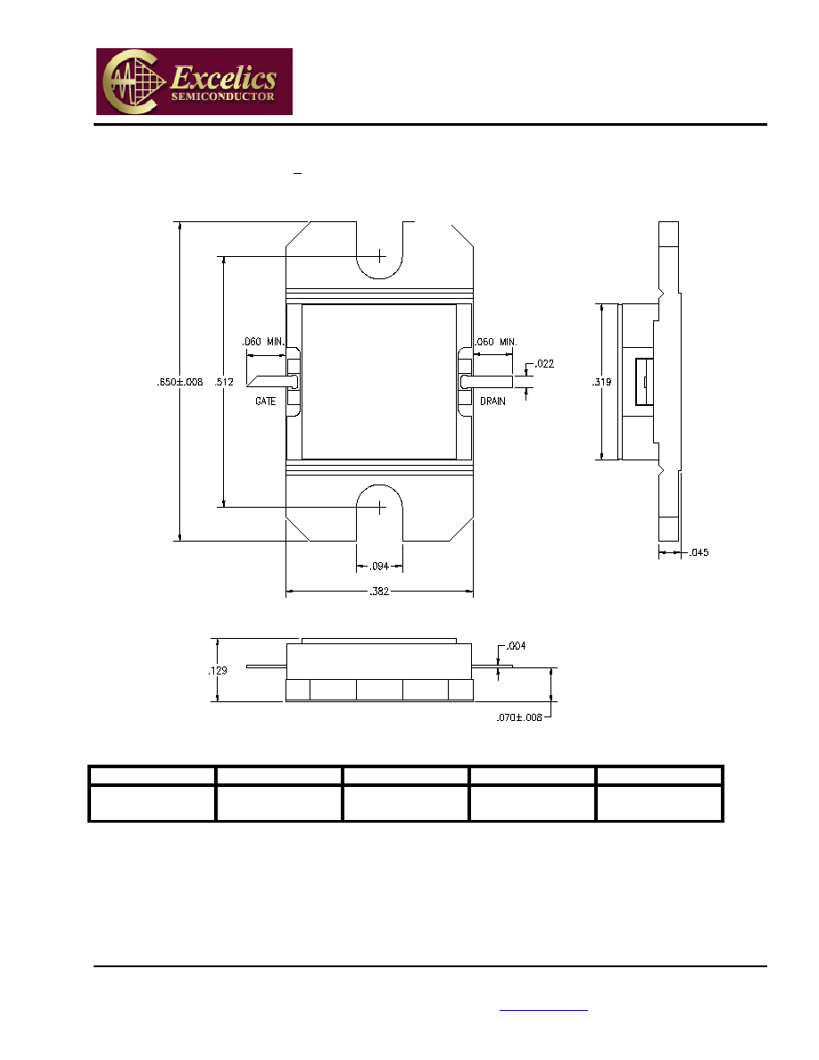
PACKAGE OUTLINE
Dimensions in inches, Tolerance + .005 unless otherwise specified
Excelics
SN
YM
ORDERING INFORMATION
Part Number
Grade
1
f
Test
(GHz)
P
1dB
(min)
IM
3
(min)
2
EIC1213-4 Industrial
12.7-13.2
GHz 35.5
-42
Notes: 1. Contact factory for military and hi-rel grades.
2. Exact test conditions are specified in "Electrical Characteristics" table.
EIC1213-4
SOURCE