EIC1415-3
UPDATED
11/22/2004
14.40 ≠ 15.35GHz 3-Watt Internally Matched Power FET
Specifications are subject to change without notice.
Excelics Semiconductor, Inc. 310 De Guigne Drive, Sunnyvale, CA 94085
page 1 of 1
Phone: 408-737-1711 Fax: 408-737-1868 Web:
www.excelics.com
Revised December 2004
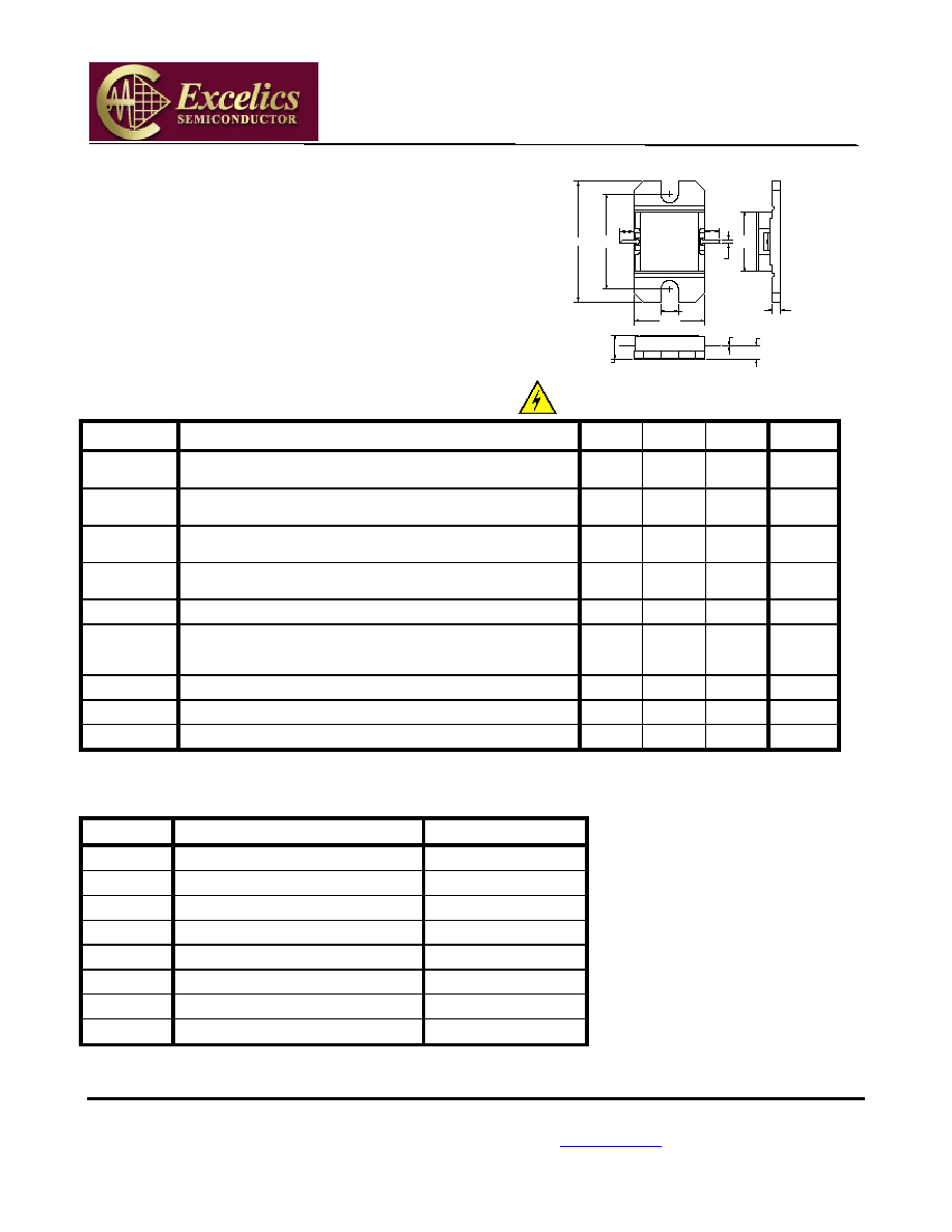
ALL DIMENSIONS IN INCHES
.512
.382
.094
Excelics
.650±.008
.129
SN
GATE
YM
.060 MIN.
.045
.070 ±.008
.004
.022
.060 MIN.
DRAIN
.319
FEATURES
∑
14.40-15.35 GHz Bandwidth
∑
Input/Output Impedance Matched to 50 Ohms
∑
+34.5 dBm Output Power at 1dB Compression
∑
6.0 dB Power Gain at 1dB Compression
∑
25% Power Added Efficiency
∑
-42 dBc IM3 at Po = 23.5 dBm SCL
∑
Hermetic Metal Flange Package
∑
100% Tested for DC, RF, and R
TH
ELECTRICAL CHARACTERISTICS (T
a
= 25
∞
C)
Caution! ESD sensitive device.
SYMBOL PARAMETERS/TEST
CONDITIONS
1
MIN
TYP
MAX
UNITS
P
1dB
Output Power at 1dB Compression f = 14.40-15.35GHz
V
DS
= 10 V, I
DSQ
800mA
33.5 34.5
dBm
G
1dB
Gain at 1dB Compression f = 14.40-15.35GHz
V
DS
= 10 V, I
DSQ
800mA
5.0 6.0 dB
G
Gain Flatness f = 14.40-15.35GHz
V
DS
= 10 V, I
DSQ
800mA
±0.6
dB
PAE
Power Added Efficiency at 1dB Compression
V
DS
= 10 V, I
DSQ
800mA f = 14.40-15.35GHz
25 %
Id
1dB
Drain Current at 1dB Compression f = 14.40-15.35GHz
900
1100
mA
IM3
Output 3rd Order Intermodulation Distortion
f = 10 MHz 2-Tone Test; Pout = 23.5 dBm S.C.L
2
V
DS
= 10 V, I
DSQ
65% IDSS
f = 15.35GHz
-38 -42
*
dBc
I
DSS
Saturated Drain Current
V
DS
= 3 V, V
GS
= 0 V
1400
1800
mA
V
P
Pinch-off Voltage
V
DS
= 3 V, I
DS
= 15 mA
-2.5
-4.0
V
R
TH
Thermal Resistance
3
8.0
9.0
o
C/W
Notes:
1.
Tested with 100 Ohm gate resistor. 2. S.C.L. = Single Carrier Level. 3. Overall Rth depends on case mounting.
* These devices are available screened for IM3 performance. Please contact factory with your requirement.
ABSOLUTE MAXIMUM RATINGS FOR CONTINUOUS OPERATION
1,2
SYMBOL CHARACTERISTIC
VALUE
V
DS
Drain to Source Voltage
10 V
V
GS
Gate to Source Voltage
-4.5 V
I
DS
Drain
Current
IDSS
I
GSF
Forward Gate Current
30 mA
P
IN
Input Power
@ 3dB compression
P
T
Total Power Dissipation
14 W
T
CH
Channel
Temperature
150∞C
T
STG
Storage
Temperature
-65/+150∞C
Notes:
1.
Operating the device beyond any of the above ratings may result in permanent damage or reduction of MTTF.
2.
Bias conditions must also satisfy the following equation P
T
< (T
CH
≠T
PKG
)/R
TH
; where T
PKG
= temperature of package, and P
T
= (V
DS
* I
DS
) ≠ (P
OUT
≠ P
IN
).
EIC1415-3