 | –≠–ª–µ–∫—Ç—Ä–æ–Ω–Ω—ã–π –∫–æ–º–ø–æ–Ω–µ–Ω—Ç: EIC5964-8 | –°–∫–∞—á–∞—Ç—å:  PDF PDF  ZIP ZIP |
EIC5964-8
Specifications are subject to change without notice.
Excelics Semiconductor, Inc. 310 De Guigne Drive, Sunnyvale, CA 94085
page 1 of 4
Phone: 408-737-1711 Fax: 408-737-1868 Web:
www.excelics.com
Revised October 2003
5.90-6.40 GHz 8-Watt Internally-Matched Power FET
FEATURES
∑
5.90 ≠ 6.40 GHz Bandwidth
∑
Input/Output Impedance Matched to 50 Ohms
∑
+39.5 dBm Output Power at 1dB Compression
∑
10.0 dB Power Gain at 1dB Compression
∑
37% Power Added Efficiency
∑
-46 dBc IM3 at Po = 28.5 dBm SCL
∑
Hermetic Metal Flange Package
∑
100% Tested for DC, RF, and R
TH
DESCRIPTION
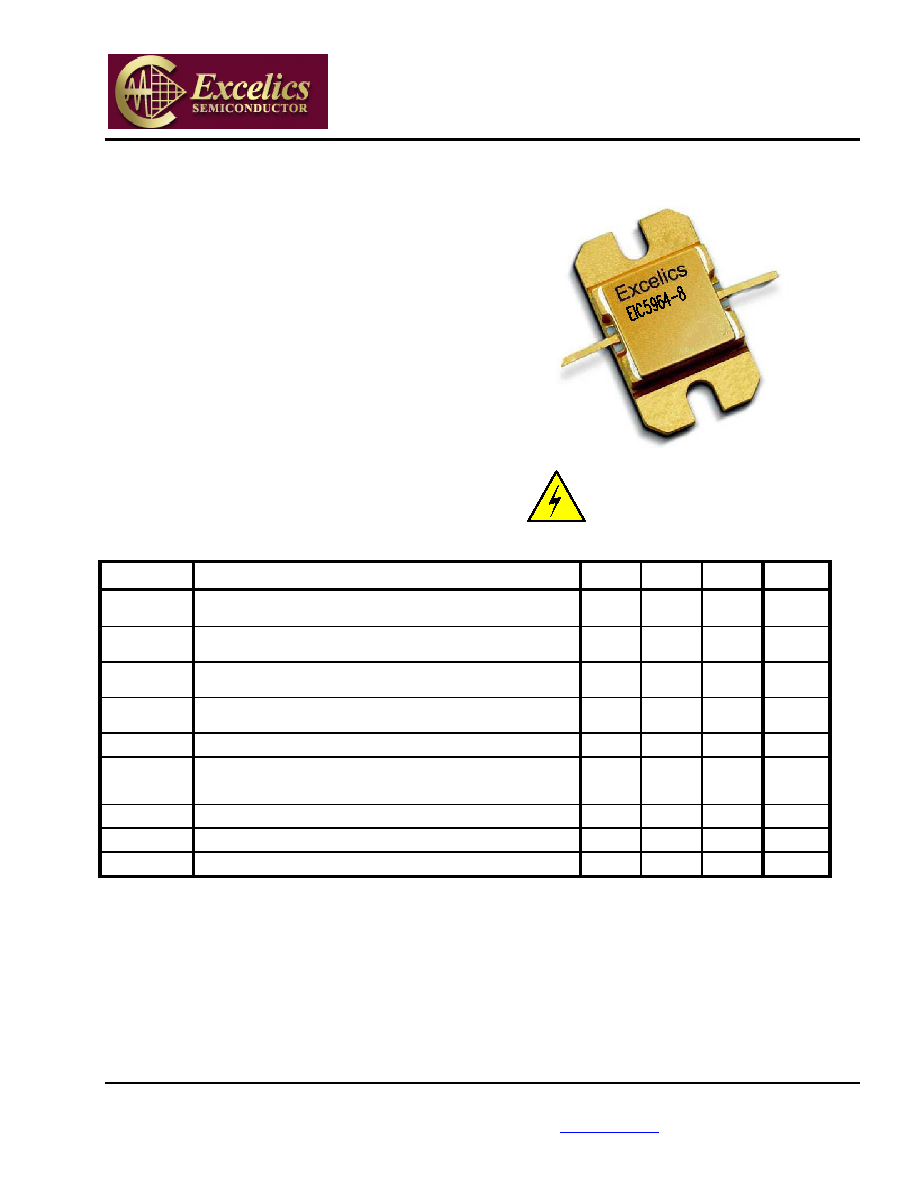
The EIC5964-8 is a high power, highly linear,
single stage MFET amplifier in a flange mount
package. This amplifier features Excelics' unique
MESFET transistor technology.
Caution! ESD sensitive device.
ELECTRICAL CHARACTERISTICS (T
a
= 25
∞
C)
SYMBOL PARAMETERS/TEST
CONDITIONS
1
MIN
TYP
MAX
UNITS
P
1dB
Output Power at 1dB Compression f = 5.90-6.40GHz
V
DS
= 10 V, I
DSQ
2200mA
38.5 39.5
dBm
G
1dB
Gain at 1dB Compression f = 5.90-6.40GHz
V
DS
= 10 V, I
DSQ
2200mA
9 10 dB
G
Gain Flatness f = 5.90-6.40GHz
V
DS
= 10 V, I
DSQ
2200mA
±0.6
dB
PAE
Power Added Efficiency at 1dB Compression
V
DS
= 10 V, I
DSQ
2200mA f = 5.90-6.40GHz
37 %
Id
1dB
Drain Current at 1dB Compression f = 5.90-6.40GHz
2200
2600
mA
IM3
Output 3rd Order Intermodulation Distortion
f = 10 MHz 2-Tone Test; Pout = 28.5 dBm S.C.L
2
V
DS
= 10 V, I
DSQ
65% IDSS f = 6.40 GHz
-43 -46 dBc
I
DSS
Saturated Drain Current
V
DS
= 3 V, V
GS
= 0 V
4000
4500
mA
V
P
Pinch-off Voltage
V
DS
= 3 V, I
DS
= 40 mA
-2.5
-4.0
V
R
TH
Thermal Resistance
3
3.5
4.0
o
C/W
Notes:
1.
Tested with 100 Ohm gate resistor.
2.
S.C.L. = Single Carrier Level.
3.
Overall Rth depends on case mounting.
EIC5964-8
Specifications are subject to change without notice.
Excelics Semiconductor, Inc. 310 De Guigne Drive, Sunnyvale, CA 94085
page 2 of 4
Phone: 408-737-1711 Fax: 408-737-1868 Web:
www.excelics.com
Revised October 2003
5.7
6
6.3
6.6
Frequency (GHz)
S21 and S12
-30
-20
-10
0
10
20
S
2
1 an
d
S
1
2 (
d
B
)
DB(|S[2,1]|)
EIC5964-8
DB(|S[1,2]|)
EIC5964-8
ABSOLUTE MAXIMUM RATINGS FOR CONTINUOUS OPERATION
1,2
SYMBOL CHARACTERISTIC
VALUE
V
DS
Drain to Source Voltage
10 V
V
GS
Gate to Source Voltage
-4.5 V
I
DS
Drain
Current
IDSS
I
GSF
Forward Gate Current
80 mA
P
IN
Input Power
@ 3dB compression
P
T
Total Power Dissipation
32 W
T
CH
Channel
Temperature
150∞C
T
STG
Storage
Temperature
-65/+150∞C
Notes:
1.
Operating the device beyond any of the above ratings may result in permanent damage or reduction of MTTF.
2.
Bias conditions must also satisfy the following equation P
T
< (T
CH
≠T
PKG
)/R
TH
; where T
PKG
= temperature of package, and
P
T
= (V
DS
* I
DS
) ≠ (P
OUT
≠ P
IN
).
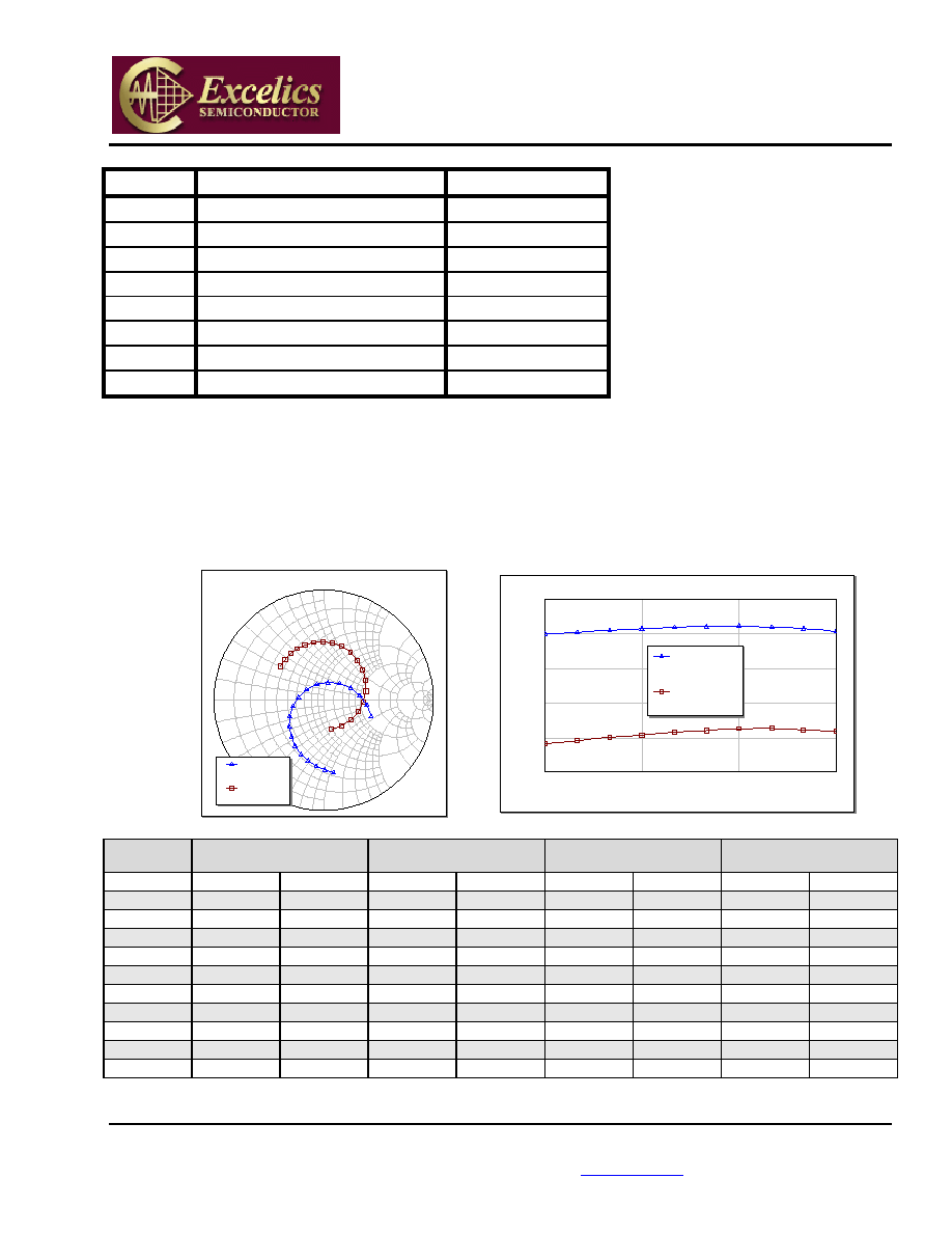
PERFORMANCE DATA
Typical S-Parameters (T= 25∞C, 50
system, de-embedded to edge of package)
V
DS
= 10 V, I
DSQ
2200mA
0
1.
0
1.0
-1.
0
10
.0
10.0
-1
0.0
5.
0
5.0
-5
.0
2.
0
2.
0
-2
.0
3.
0
3.
0
-3
.0
4.
0
4.
0
-4
.0
0.
2
0.
2
-0.
2
0.
4
0.
4
-0
.4
0.
6
0.
6
-0
.6
0.
8
0
.
8
-
0
.8
S11 and S22
Swp Max
6.6GHz
Swp Min
5.7GHz
S[1,1]
EIC5964-8
S[2,2]
EIC5964-8
FREQ
--- S11 ---
--- S21 ---
--- S12 ---
--- S22 ---
(GHz)
MAG
ANG
MAG
ANG
MAG
ANG
MAG
ANG
5.0 0.873 -7.73
1.9865
102.43 0.0385 50.45 0.4069 -90.78
5.2
0.8439
-25.93
2.285
77.92
0.0467
23.43
0.4003
-128.98
5.4 0.7893
-46.35
2.6094 51.4 0.0592 -4.16 0.4285 -166.69
5.6
0.7151
-69.29
2.9628
23.77
0.0737
-33.07
0.4765
158.39
5.8 0.6028
-96.47
3.3734 -5.88 0.0912 -62.69 0.5213 125.52
6.0
0.444
-131.54
3.7964
-39.07
0.1107
-96.25
0.5321
90.88
6.2 0.2308 173.31 4.0744 -76.09 0.1282 -133.24 0.4733 49.87
6.4
0.2091
46.37
4.0033
-116.4
0.1362
-173.52
0.3603
-2.01
6.6 0.455 -18.8
3.4617
-156.9 0.1237 147.8 0.2712 -75.07
6.8
0.6333
-56.77
2.6951
167.51
0.1009
112.66
0.3134
-142.54
7.0 0.7311
-85.42 2.035 136.97 0.0814 83.64 0.4055 176.45
EIC5964-8
Specifications are subject to change without notice.
Excelics Semiconductor, Inc. 310 De Guigne Drive, Sunnyvale, CA 94085
page 3 of 4
Phone: 408-737-1711 Fax: 408-737-1868 Web:
www.excelics.com
Revised October 2003
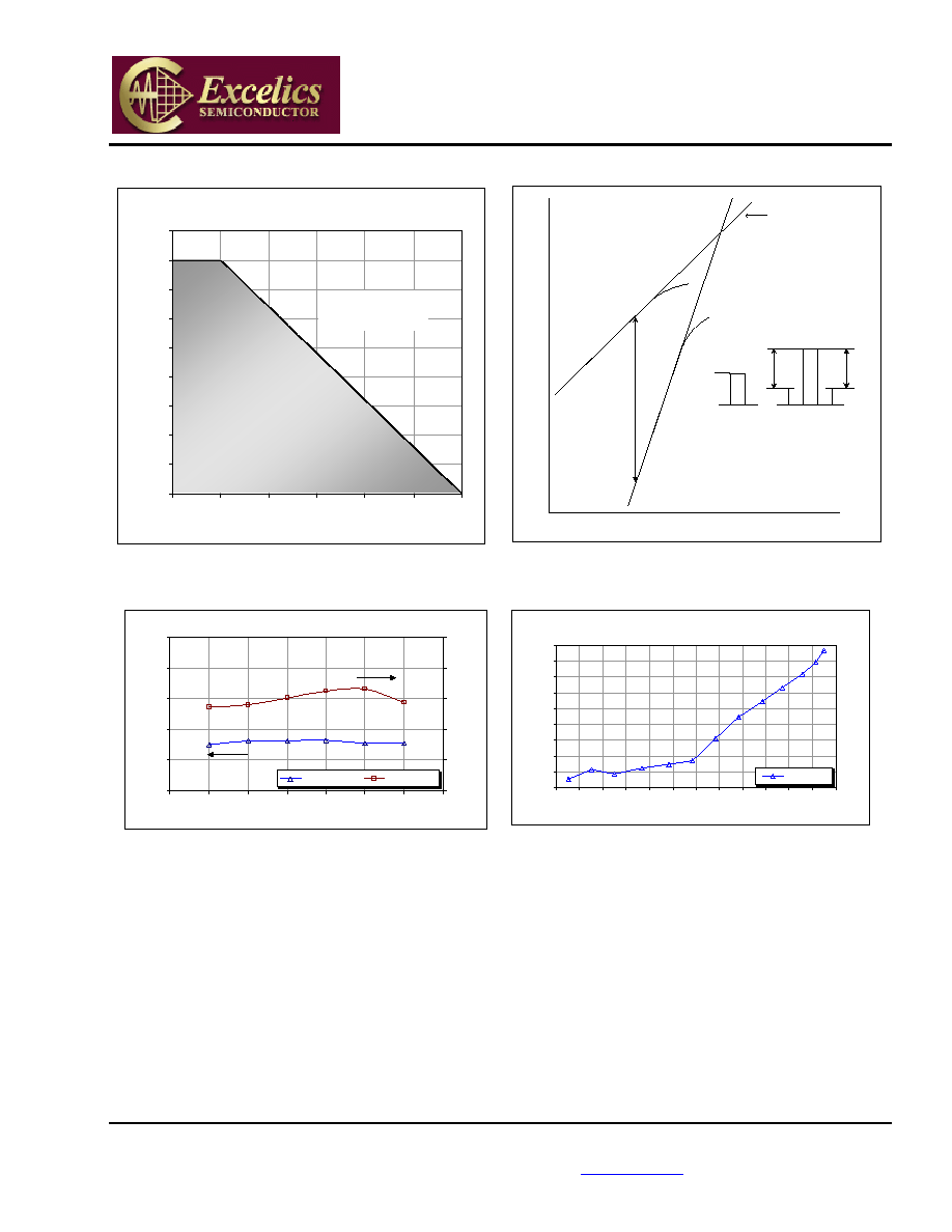
Power De-rating Curve and IM3 Definition
Power Dissipation vs. Temperature
0
4
8
12
16
20
24
28
32
36
0
25
50
75
100
125
150
Case Temperature (∞C)
T
o
t
a
l
P
o
w
e
r
D
i
s
s
i
pat
i
on (
W
)
Safe Operating
Region
Potentially Unsafe
Operating Region
f1 f2
(2f1-f2) f1 f2 (2f2-f1)
IM3
Pout
Pin
IP
3
= Pout + IM3/2
THIRD-ORDER
INTERCEPT POINT IP3
f1 or f2
(2f2 - f1) or (2f1 - f2)
Pin [S.C.L.] (dBm)
P
o
u
t
[S
.C
.L
.
]
(
d
B
m
)
IM3
Typical Power Data (V
DS
= 10 V, I
DSQ
= 2200 mA)
Typical IM3 Data (V
DS
= 10 V,
I
DSQ
65% IDSS
)
P-1dB & G-1dB vs Frequency
38
39
40
41
42
43
5.8
5.9
6.0
6.1
6.2
6.3
6.4
6.5
Frequency (GHz)
P
-
1
d
B (d
Bm
)
8
9
10
11
12
13
G
-
1dB
(
d
B
)
P-1dB (dBm)
G-1dB (dB)
IM3 vs Output Power
f1 = 6.40 GHz, f2 = 6.41 GHz
-60
-55
-50
-45
-40
-35
-30
-25
-20
-15
23
24
25
26
27
28
29
30
31
32
33
34
35
Pout [S.C.L.] (dBm)
IM
3
(
d
B
c
)
IM3 (dBc)
EIC5964-8
Specifications are subject to change without notice.
Excelics Semiconductor, Inc. 310 De Guigne Drive, Sunnyvale, CA 94085
page 4 of 4
Phone: 408-737-1711 Fax: 408-737-1868 Web:
www.excelics.com
Revised October 2003
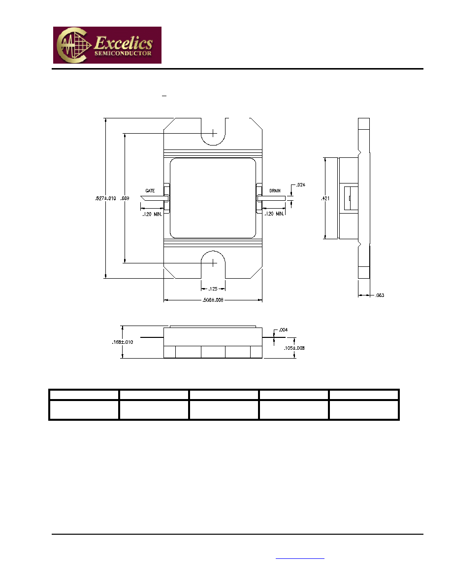
PACKAGE OUTLINE
Dimensions in inches, Tolerance + .005 unless otherwise specified
SN
Excelics
YM
ORDERING INFORMATION
Part Number
Grade
1
f
Test
(GHz)
P
1dB
(min)
IM
3
(min)
2
EIC5964-8 Industrial 5.9-6.4
GHz 38.5
-43
Notes: 1. Contact factory for military and hi-rel grades.
2. Exact test conditions are specified in "Electrical Characteristics" table.
EIC5964-8
SOURCE