 | –≠–ª–µ–∫—Ç—Ä–æ–Ω–Ω—ã–π –∫–æ–º–ø–æ–Ω–µ–Ω—Ç: EIC7785-5 | –°–∫–∞—á–∞—Ç—å:  PDF PDF  ZIP ZIP |
EIC7785-5
Specifications are subject to change without notice.
Excelics Semiconductor, Inc. 310 De Guigne Drive, Sunnyvale, CA 94085
page 1 of 4
Phone: 408-737-1711 Fax: 408-737-1868 Web:
www.excelics.com
Revised October 2003
7.7-8.5 GHz 5-Watt Internally-Matched Power FET
FEATURES
∑
7.7 ≠ 8.5 GHz Bandwidth
∑
Input/Output Impedance Matched to 50 Ohms
∑
+37.5 dBm Output Power at 1dB Compression
∑
8.5 dB Power Gain at 1dB Compression
∑
34% Power Added Efficiency
∑
-49 dBc IM3 at Po = 26.5 dBm SCL
∑
Hermetic Metal Flange Package
∑
100% Tested for DC, RF, and R
TH
DESCRIPTION
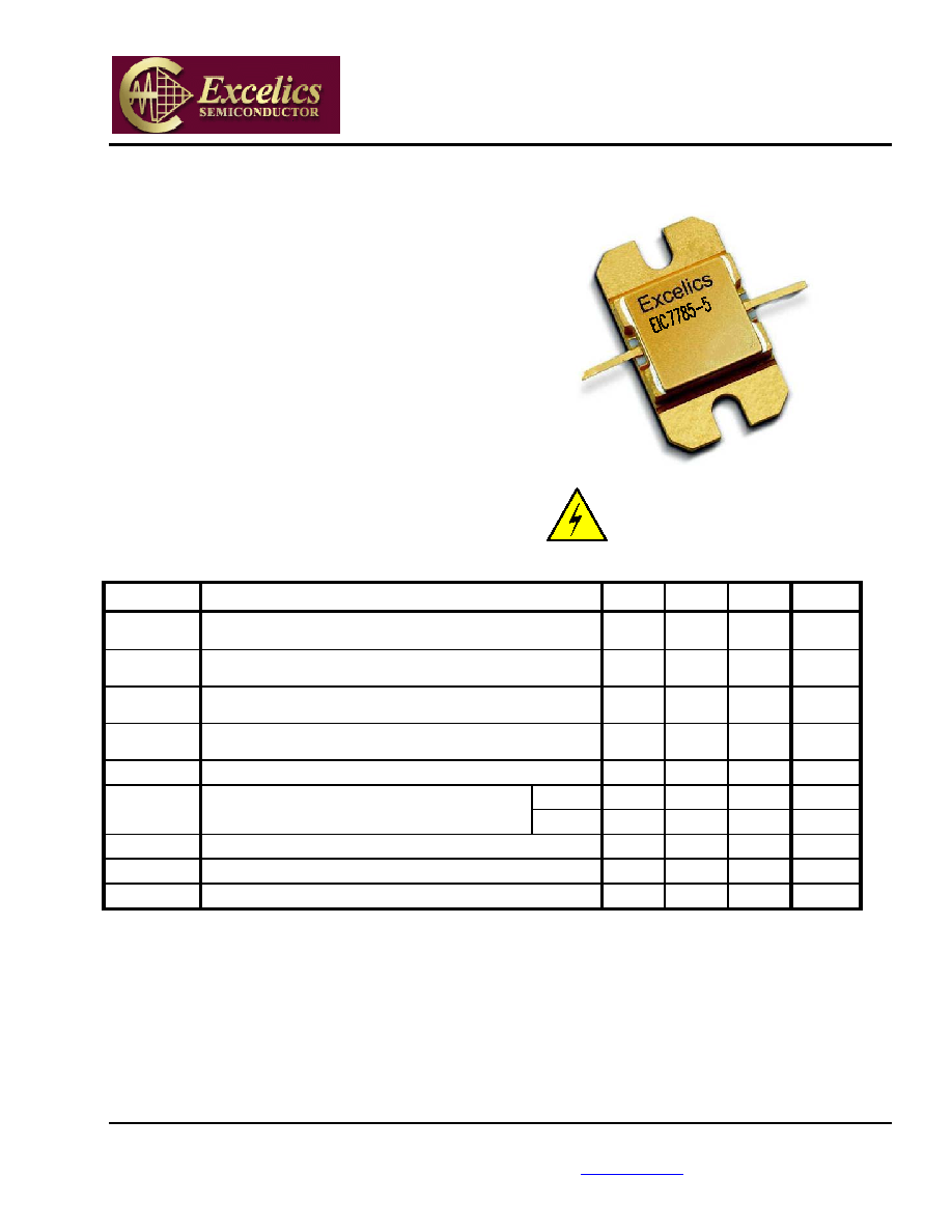
The EIC7785-5 is a high power, highly linear,
single stage MFET amplifier in a flange mount
package. This amplifier features Excelics' unique
MESFET transistor technology.
Caution! ESD sensitive device.
ELECTRICAL CHARACTERISTICS (T
a
= 25
∞
C)
SYMBOL PARAMETERS/TEST
CONDITIONS
1
MIN
TYP
MAX
UNITS
P
1dB
Output Power at 1dB Compression f = 7.7-8.5 GHz
V
DS
= 10 V, I
DSQ
1600mA
36.5 37.5
dBm
G
1dB
Gain at 1dB Compression
f = 7.7-8.5 GHz
V
DS
= 10 V, I
DSQ
1600mA
7.5 8.5 dB
G
Gain Flatness f = 7.7-8.5 GHz
V
DS
= 10 V, I
DSQ
1600mA
±0.6
dB
PAE
Power Added Efficiency at 1dB Compression
V
DS
= 10 V, I
DSQ
1600mA
f = 7.7-8.5 GHz
34 %
Id
1dB
Drain Current at 1dB Compression
f = 7.7-8.5 GHz
1600
1900
mA
Opt-01
-42 -45 dBc
IM3
Output 3rd Order Intermodulation Distortion
f = 10 MHz 2-Tone Test; Pout = 26.5 dBm S.C.L
2
V
DS
= 10 V, I
DSQ
65% IDSS f = 8.5 GHz
Opt-02
-46 -49 dBc
I
DSS
Saturated Drain Current
V
DS
= 3 V, V
GS
= 0 V
2900
3500
mA
V
P
Pinch-off Voltage
V
DS
= 3 V, I
DS
= 30 mA
-2.5
-4.0
V
R
TH
Thermal Resistance
3
5.0
5.5
o
C/W
Notes:
1.
Tested with 100 Ohm gate resistor.
2.
S.C.L. = Single Carrier Level.
3.
Overall Rth depends on case mounting.
EIC7785-5
Specifications are subject to change without notice.
Excelics Semiconductor, Inc. 310 De Guigne Drive, Sunnyvale, CA 94085
page 2 of 4
Phone: 408-737-1711 Fax: 408-737-1868 Web:
www.excelics.com
Revised October 2003
7.5
7.8
8.1
8.4
8.7
Frequency (GHz)
S21 and S12
-30
-20
-10
0
10
S
21 and S
12 (
d
B
)
DB(|S[2,1]|)
EIC7785-5
DB(|S[1,2]|)
EIC7785-5
ABSOLUTE MAXIMUM RATINGS FOR CONTINUOUS OPERATION
1,2
SYMBOL CHARACTERISTIC
VALUE
V
DS
Drain to Source Voltage
10 V
V
GS
Gate to Source Voltage
-4.5 V
I
DS
Drain
Current
IDSS
I
GSF
Forward Gate Current
60 mA
P
IN
Input Power
@ 3dB compression
P
T
Total Power Dissipation
23 W
T
CH
Channel
Temperature
150∞C
T
STG
Storage
Temperature
-65/+150∞C
Notes:
1.
Operating the device beyond any of the above ratings may result in permanent damage or reduction of MTTF.
2.
Bias conditions must also satisfy the following equation P
T
< (T
CH
≠T
PKG
)/R
TH
; where T
PKG
= temperature of package, and
P
T
= (V
DS
* I
DS
) ≠ (P
OUT
≠ P
IN
).
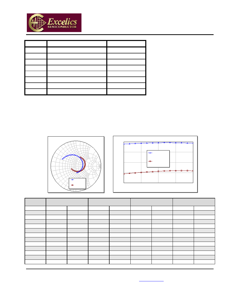
PERFORMANCE DATA
Typical S-Parameters (T= 25∞C, 50
system, de-embedded to edge of package)
V
DS
= 10 V, I
DSQ
1600mA
0
1.0
1.0
-1.
0
10.0
10.0
-1
0.0
5.0
5.0
-5
.0
2.0
2.
0
-2
.0
3.0
3.
0
-3
.0
4.0
4.
0
-4
.0
0.2
0.
2
-0.
2
0.4
0.
4
-0
.4
0.6
0.
6
-0
.6
0.8
0
.
8
-
0
.8
S11 and S22
Swp Max
8.7GHz
Swp Min
7.5GHz
S[1,1]
EIC7785-5
S[2,2]
EIC7785-5
FREQ
--- S11 ---
--- S21 ---
--- S12 ---
--- S22 ---
(GHz)
MAG
ANG
MAG
ANG
MAG
ANG
MAG
ANG
7.5 0.6072 151.65 2.4887 -96.64 0.0877 -140.79 0.3974 63.69
7.6
0.5668
139.93
2.5636
-108.26
0.0935
-152.21
0.399
51.15
7.7 0.5301 127.41 2.6446 -120.35 0.0984 -164.2 0.3981 38.7
7.8
0.4896
113.26
2.7096
-132.52
0.1039
-176.06
0.392
26.7
7.9
0.4497
98.49
2.7726
-145.04
0.1085
171.35
0.378
14.39
8
0.4085
82.47
2.8207
-157.79
0.1123
158.96
0.3592
1.76
8.1 0.3689
64.87 2.8563
-170.82 0.1168 146.5 0.3329 -11.65
8.2
0.331
45.51
2.8892
175.98
0.1211
133.84
0.3001
-26.37
8.3 0.2961
23.89 2.888 162.68
0.1237 121.11 0.2676 -43.46
8.4
0.2689
-0.24
2.8767
149.22
0.1251
107.74
0.2323
-63
8.5 0.2517
-26.44
2.8389
135.66 0.1254 94.86 0.2034 -87.46
8.6
0.2485
-54.31
2.7741
122.25
0.1254
81.38
0.1942
-116.35
8.7 0.2603 -81 2.7202
108.74
0.1226 67.75 0.2049 -145.47
EIC7785-5
Specifications are subject to change without notice.
Excelics Semiconductor, Inc. 310 De Guigne Drive, Sunnyvale, CA 94085
page 3 of 4
Phone: 408-737-1711 Fax: 408-737-1868 Web:
www.excelics.com
Revised October 2003
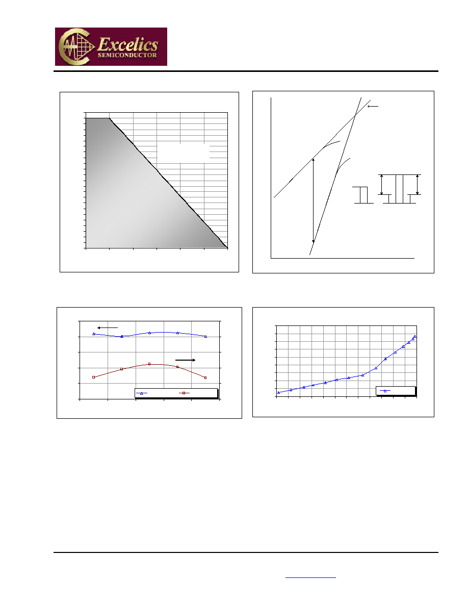
Power De-rating Curve and IM3 Definition
Power Dissipation vs. Temperature
0
1
2
3
4
5
6
7
8
9
10
11
12
13
14
15
16
17
18
19
20
21
22
23
24
0
25
50
75
100
125
150
Case Temperature (∞C)
T
o
t
a
l
P
o
we
r
Di
s
s
i
p
a
t
i
o
n
(
W
)
Safe Operating
Region
Potentially Unsafe
Operating Region
f1 f2
(2f1-f2) f1 f2 (2f2-f1)
IM3
Pout
Pin
IP
3
= Pout + IM3/2
THIRD-ORDER
INTERCEPT POINT IP3
f1 or f2
(2f2 - f1) or (2f1 - f2)
Pin [S.C.L.] (dBm)
P
out
[
S
.C
.
L
.]
(
d
Bm)
IM3
Typical Power Data (V
DS
= 10 V, I
DSQ
= 1600 mA)
Typical IM3 Data (V
DS
= 10 V,
I
DSQ
65% IDSS
)
P-1dB & G-1dB vs Frequency
34
35
36
37
38
39
7.6
7.8
8.0
8.2
8.4
8.6
Frequency (GHz)
P
-
1dB
(
d
B
m
)
6
7
8
9
10
11
G
-
1dB
(
d
B
)
P-1dB (dBm)
G-1dB (dB)
IM3 vs Output Power
f1 = 8.50 GHz, f2 = 8.51 GHz
-60
-55
-50
-45
-40
-35
-30
-25
-20
-15
21
22
23
24
25
26
27
28
29
30
31
32
33
Pout [S.C.L.] (dBm)
IM
3
(
d
B
c
)
IM3 (dBc)
EIC7785-5
Specifications are subject to change without notice.
Excelics Semiconductor, Inc. 310 De Guigne Drive, Sunnyvale, CA 94085
page 4 of 4
Phone: 408-737-1711 Fax: 408-737-1868 Web:
www.excelics.com
Revised October 2003
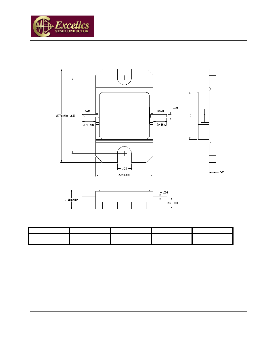
PACKAGE OUTLINE
Dimensions in inches, Tolerance + .005 unless otherwise specified
SN
Excelics
YM
ORDERING INFORMATION
Part Number
Grade
1
f
Test
(GHz)
P
1dB
(min)
IM
3
(min)
2
EIC7785-5-01 Industrial 7.7-8.5
GHz
36.5
-42
EIC7785-5-02 Industrial 7.7-8.5
GHz
36.5
-46
Notes: 1. Contact factory for military and hi-rel grades.
2. Exact test conditions are specified in "Electrical Characteristics" table.
EIC7785-5
SOURCE