EIC8596-8
Specifications are subject to change without notice.
Excelics Semiconductor, Inc. 310 De Guigne Drive, Sunnyvale, CA 94085
page 1 of 4
Phone: 408-737-1711 Fax: 408-737-1868 Web:
www.excelics.com
Revised July 2004
8.50-9.60 GHz 8-Watt Internally-Matched Power FET
Issued Date: 06-07-04
FEATURES
�
8.50 � 9.60 GHz Bandwidth
�
Input/Output Impedance Matched to 50 Ohms
�
+39.5 dBm Output Power at 1dB Compression
�
7.5 dB Power Gain at 1dB Compression
�
30% Power Added Efficiency
�
-43 dBc IM3 at Po = 28.5 dBm SCL
�
Hermetic Metal Flange Package
�
100% Tested for DC, RF, and R
TH
DESCRIPTION
The EIC8596-8 is a high power, highly linear,
single stage MFET amplifier in a flange mount
package. This amplifier features Excelics' unique
MESFET transistor technology.
Caution! ESD sensitive device.
ELECTRICAL CHARACTERISTICS (T
a
= 25
�
C)
SYMBOL PARAMETERS/TEST
CONDITIONS
1
MIN
TYP
MAX
UNITS
P
1dB
Output Power at 1dB Compression f = 8.50-9.60GHz
V
DS
= 10 V, I
DSQ
2200mA
38.5 39.5
dBm
G
1dB
Gain at 1dB Compression f = 8.50-9.60GHz
V
DS
= 10 V, I
DSQ
2200mA
6.5 7.5 dB
G
Gain Flatness f = 8.50-9.60GHz
V
DS
= 10 V, I
DSQ
2200mA
�0.6
dB
PAE
Power Added Efficiency at 1dB Compression
V
DS
= 10 V, I
DSQ
2200mA f = 8.50-9.60GHz
30 %
Id
1dB
Drain Current at 1dB Compression f = 8.50-9.60GHz
2200
2600
mA
IM3
Output 3rd Order Intermodulation Distortion
f = 10 MHz 2-Tone Test; Pout = 28.5 dBm S.C.L
2
V
DS
= 10 V, I
DSQ
65% IDSS f = 9.60 GHz
-40 -43 dBc
I
DSS
Saturated Drain Current
V
DS
= 3 V, V
GS
= 0 V
3700
4300
mA
V
P
Pinch-off Voltage
V
DS
= 3 V, I
DS
= 40 mA
-2.5
-4.0
V
R
TH
Thermal Resistance
3
2.5
3.5
o
C/W
Notes:
1.
Tested with 100 Ohm gate resistor.
2.
S.C.L. = Single Carrier Level.
3.
Overall Rth depends on case mounting.
EIC8596-8
Specifications are subject to change without notice.
Excelics Semiconductor, Inc. 310 De Guigne Drive, Sunnyvale, CA 94085
page 2 of 4
Phone: 408-737-1711 Fax: 408-737-1868 Web:
www.excelics.com
Revised July 2004
ABSOLUTE MAXIMUM RATINGS FOR CONTINUOUS OPERATION
1,2
SYMBOL CHARACTERISTIC
VALUE
V
DS
Drain to Source Voltage
10 V
V
GS
Gate to Source Voltage
-4.5 V
I
DS
Drain
Current
IDSS
I
GSF
Forward Gate Current
80 mA
P
IN
Input Power
@ 3dB compression
P
T
Total Power Dissipation
35 W
T
CH
Channel
Temperature
150�C
T
STG
Storage
Temperature
-65/+150�C
Notes:
1.
Operating the device beyond any of the above ratings may result in permanent damage or reduction of MTTF.
2.
Bias conditions must also satisfy the following equation P
T
< (T
CH
�T
PKG
)/R
TH
; where T
PKG
= temperature of package, and
P
T
= (V
DS
* I
DS
) � (P
OUT
� P
IN
).
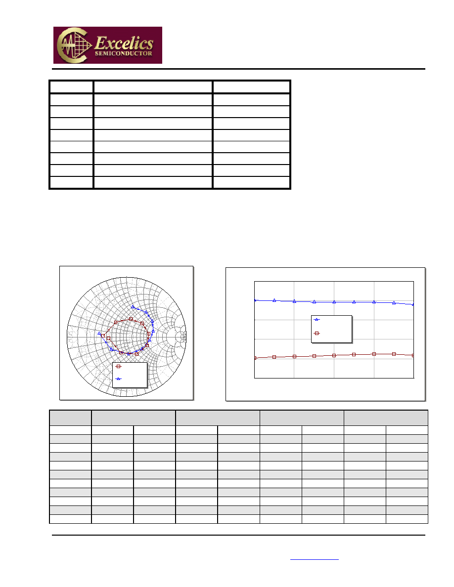
PERFORMANCE DATA
Typical S-Parameters (T= 25�C, 50
system, de-embedded to edge of package)
V
DS
= 10 V, I
DSQ
2200mA
FREQ
--- S11 ---
--- S21 ---
--- S12 ---
--- S22 ---
(GHz)
MAG
ANG
MAG
ANG
MAG
ANG
MAG
ANG
8.00 0.390
177.400
3.255
-57.380 0.105 -114.220 0.514 78.300
8.25
0.306
125.970
3.195
-88.570
0.112
-145.020
0.527
51.750
8.50 0.309 77.020 3.052
-116.850 0.113 -173.180 0.507 31.300
8.75
0.348
40.380
2.957
-144.300
0.117
161.600
0.459
12.160
9.00 0.378 8.330 2.917
-170.590 0.122 135.400 0.393 -8.460
9.25
0.371
-22.220
2.884
161.430
0.128
108.950
0.328
-38.080
9.50 0.334 -59.000 2.897 132.320 0.131 81.650 0.287 -82.820
9.75
0.280
-109.930
2.793
100.510
0.132
49.430
0.327
-140.430
10.00 0.299
-175.540
2.528 66.690 0.122 16.320 0.462 172.730
10.25
0.387
132.770
2.112
34.290
0.103
-16.260
0.614
140.720
10.50 0.490 98.340 1.672 5.950 0.081 -45.080 0.713 117.810
0
1.0
-1.0
1.0
10.0
-10.0
10.
0
5.0
-5.0
5.0
2.0
-2
.0
2.
0
3.0
-3.
0
3.0
4.0
-4.
0
4.0
0.2
-0.
2
0.2
0.4
-0
.4
0.
4
0.6
-0
.6
0.
6
0.8
-
0
.
8
0
.
8
0
1.0
1.0
-1.0
10.0
10.0
-1
0.
0
5.0
5.0
-5.
0
2.0
2.
0
-2
.0
3.0
3.
0
-3
.0
4.0
4.
0
-4.
0
0.2
0.2
-0.
2
0.4
0.
4
-0
.4
0.6
0.
6
-0
.6
0.8
0
.
8
-
0
.
8
S11 and S22
Swp Max
10GHz
Swp Min
8GHz
S[1,1] *
EIC8596-8
S[2,2] *
EIC8596-8
8
8.5
9
9.5
10
Frequency (GHz)
S21 and S12
-30
-20
-10
0
10
20
S
2
1 and
S12
(dB)
DB(|S[2,1]|) *
EIC8596-8
DB(|S[1,2]|) *
EIC8596-8
EIC8596-8
Specifications are subject to change without notice.
Excelics Semiconductor, Inc. 310 De Guigne Drive, Sunnyvale, CA 94085
page 3 of 4
Phone: 408-737-1711 Fax: 408-737-1868 Web:
www.excelics.com
Revised July 2004
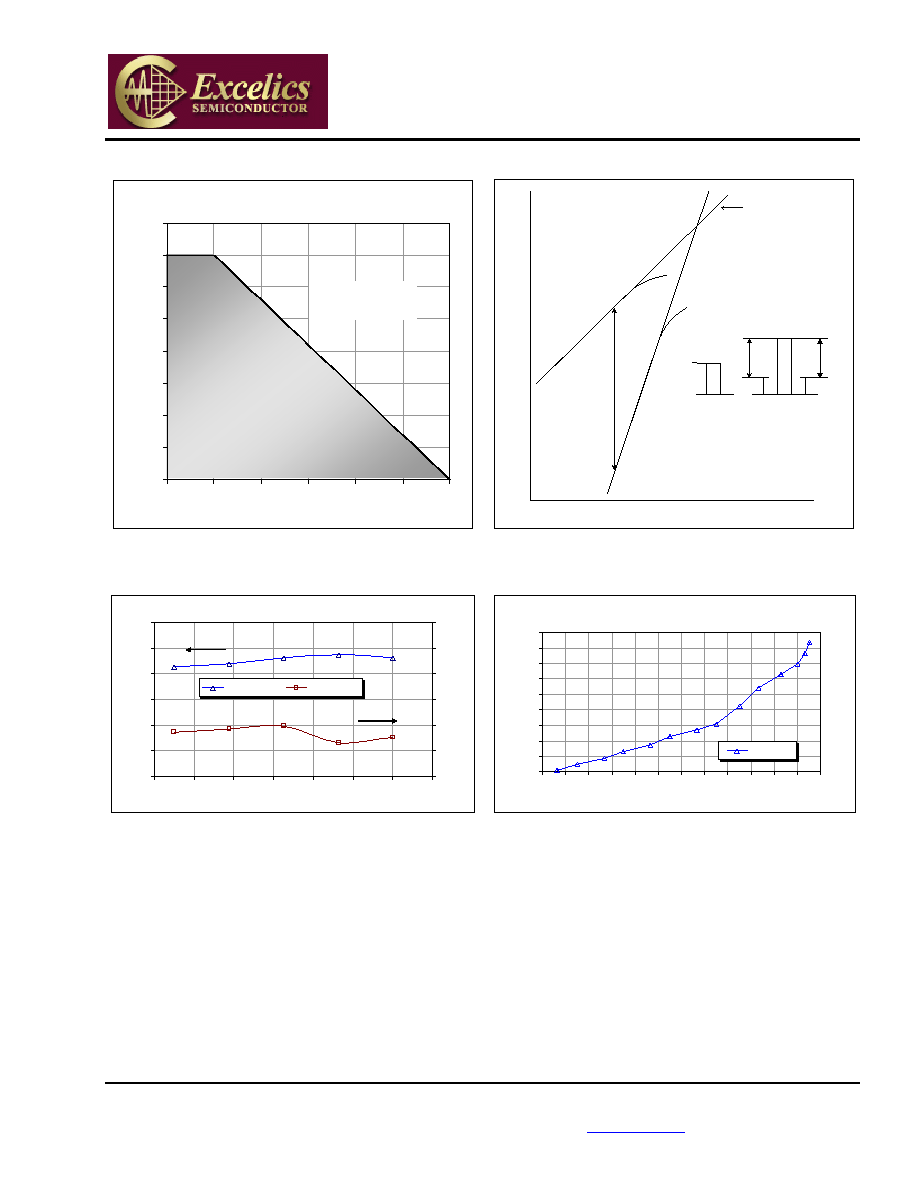
Power De-rating Curve and IM3 Definition
Power Dissipation vs. Temperature
0
5
10
15
20
25
30
35
40
0
25
50
75
100
125
150
Case Temperature (�C)
T
o
ta
l
P
o
w
e
r
D
i
s
s
i
p
a
ti
o
n
(
W
)
Safe Operating
Region
Potentially Unsafe
Operating Region
f1 f2
(2f1-f2) f1 f2 (2f2-f1)
IM3
Pout
Pin
IP
3
= Pout + IM3/2
THIRD-ORDER
INTERCEPT POINT IP3
f1 or f2
(2f2 - f1) or (2f1 - f2)
Pin [S.C.L.] (dBm)
P
o
u
t
[S
.C.L
.]
(
d
B
m
)
IM3
Typical Power Data (V
DS
= 10 V, I
DSQ
= 2200 mA)
Typical IM3 Data (V
DS
= 10 V,
I
DSQ
65% IDSS
)
P-1dB & G-1dB vs Frequency
35
36
37
38
39
40
41
8.4
8.6
8.8
9.0
9.2
9.4
9.6
9.8
Frequency (GHz)
P
-
1
d
B (d
Bm)
7
8
9
10
11
12
13
G-
1
d
B
(
d
B
)
P-1dB (dBm)
G-1dB (dB)
IM3 vs Output Power
f1 = 9.60 GHz, f2 = 9.59 GHz
-60
-55
-50
-45
-40
-35
-30
-25
-20
-15
23
24
25
26
27
28
29
30
31
32
33
34
35
Pout [S.C.L.] (dBm)
IM
3
(
d
Bc
)
IM3 (dBc)
EIC8596-8
Specifications are subject to change without notice.
Excelics Semiconductor, Inc. 310 De Guigne Drive, Sunnyvale, CA 94085
page 4 of 4
Phone: 408-737-1711 Fax: 408-737-1868 Web:
www.excelics.com
Revised July 2004
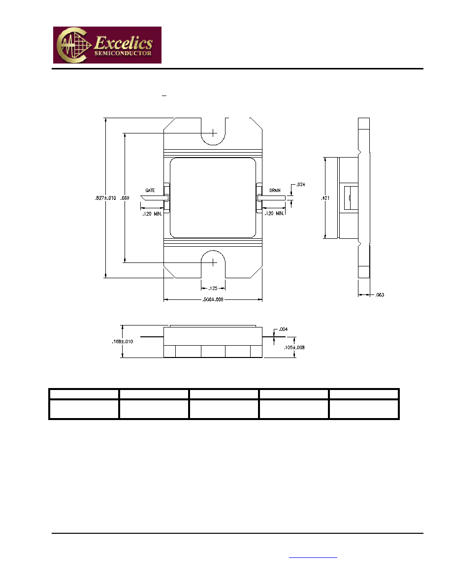
PACKAGE OUTLINE
Dimensions in inches, Tolerance + .005 unless otherwise specified
SN
Excelics
YM
ORDERING INFORMATION
Part Number
Grade
1
f
Test
(GHz)
P
1dB
(min)
IM
3
(min)
2
EIC8596-8 Industrial
8.50-9.60
GHz 38.5
-40
Notes: 1. Contact factory for military and hi-rel grades.
2. Exact test conditions are specified in "Electrical Characteristics" table.
EIC8596-8
SOURCE