RFMA5065-2W
UPDATED 09/01/2006
5.0 ≠ 6.5 GHz Power Amplifier MMIC
Specifications are subject to change without notice.
Excelics Semiconductor, Inc. 310 De Guigne Drive, Sunnyvale, CA 94085
page 1 of 2
Phone: 408-737-1711 Fax: 408-737-1868 Web:
www.excelics.com
Revised September 2006
Excelics
RFMA5065
-2W-02
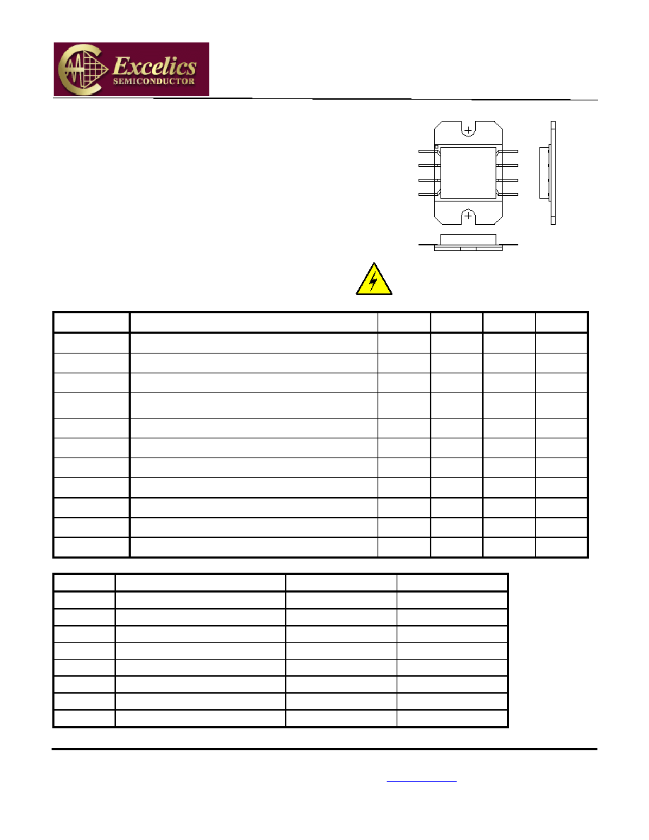
N/C
Vg
RF IN
N/C
RF OUT
N/C
N/C
Vd
FEATURES
∑
5.0 ≠ 6.5 GHz Operating Frequency Range
∑
33dBm Output Power at 1dB Compression
∑
30.0 dB Typical Power Gain @1dB gain compression
∑
-44dBc Typical OIM3 @ each tone Pout 22dBm
APPLICATIONS
∑
Point-to-point and point-to-multipoint radio
∑
Military Radar Systems
Caution! ESD sensitive device.
ELECTRICAL CHARACTERISTICS (Tb = 25
∞
C,
50 ohm, Vdd=10V, Vgg=-5V)
SYMBOL PARAMETER/TEST
CONDITIONS MIN
TYP
MAX
UNITS
F
Operating Frequency Range
5.0
6.5
GHz
P1dB
Output Power at 1dB Gain Compression
32
33
dBm
G1dB
Gain @1dB gain compression
28.0
32.0
dB
OIMD3
Output 3
rd
Order Intermodulation Distortion
@f=10MHz, Each Tone Pout 22dBm
-40 -44 dBc
Input RL
Input Return Loss
-12
-6
dB
Output RL
Output Return Loss
-6
dB
Idd
Drain Current @small signal output power level
1260
1500
mA
Vdd
Drain
Supply
Voltage
10 V
Vgg
Gate Supply Voltage
-5
V
Rth
Thermal Resistance
4
4.5
o
C/W
Tb
Operating Base Plate Temperature
- 30
+ 80
∫C
MAXIMUM RATINGS @25∞C
1,2
SYMBOL CHARACTERISTIC
ABSOLUTE CONTINUOUS
Vdd
Drain Supply Voltage
14V
10V
Vgg
Gate Supply Voltage
-10V
-5.5 V
Idq Quiescent
Drain
Current
Idss
1.5A
Igg
Gate Current
150mA
50 mA
P
IN
Input Power
8dBm
@ 3dB compression
T
CH
Channel
Temperature
175∞C
150∞C
T
STG
Storage
Temperature
-65/175∞C
-65/150∞C
Pt Total
Power
Dissipation
30W
15W
1. Operating the device beyond any of the above rating may reduce MTTF and cause permanent damage.
2. Bias conditions must also satisfy the following equation Vdd*Idd < (T
CH
≠Tb)/R
TH
RFMA5065-2W
UPDATED 09/01/2006
5.0 ≠ 6.5 GHz Power Amplifier MMIC
Specifications are subject to change without notice.
Excelics Semiconductor, Inc. 310 De Guigne Drive, Sunnyvale, CA 94085
page 2 of 2
Phone: 408-737-1711 Fax: 408-737-1868 Web:
www.excelics.com
Revised September 2006
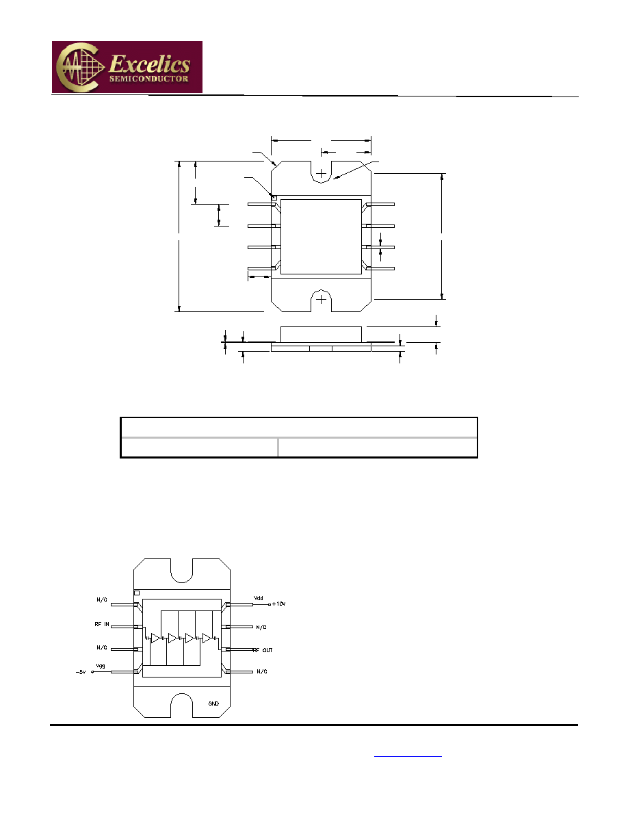
Package Dimension and Pin Assignment
-2W-02
RFMA5065
Excelics
DIMENSION: INCH
TOLERANCE: ±0.005
8X 0.004
0.040
8X 0.100±0.010
0.709
RF IN
Vg
N/C
PIN1 Indicator
0.204
6x0.100
N/C
4X.050 CHAMFER
0.075
0.025
2X DIA .090 THRU
Vd
N/C
N/C
RF OUT
8 X .013
0.591
0.216
0.433
Ordering Information
Part Number
RFMA5065-2W-02
Refer 02 Package Outline
Application Note
1. The package should be screwed onto a good heat sink and ground
2. Turn on/off sequence is required:
---to turn on: apply -5V first, then +10V.
---to turn off: turn +10V off first, then turn -5V off
3. Recommended Bias Circuit and Internal Block Diagram
"N/C" pins on package can be either
grounded or left open.
(No connection inside of package)