
E S I
E S I
1
Rev. 0B January 5 , 2006
ES29LV160E
Excel Semiconductor inc.
ES29LV160E
16Mbit(2M x 8/1M x 16)
CMOS 3.0 Volt-only, Boot Sector Flash Memory
GENERAL FEATURES
∑ Single power supply operation
- 2.7V -3.6V for read, program and erase operations
∑ Sector Structure
- 16Kbyte x 1, 8Kbyte x 2, 32Kbyte x 1 boot sectors
- 64Kbyte x 31 sectors
∑ Top or Bottom boot block
- ES29LV160ET for Top boot block device
- ES29LV160EB for Bottom boot block device
∑ Package Options
- 48-pin TSOP
- 48-ball FBGA ( 6 x 8 mm )
- Pb-free packages
- All Pb-free products are RoHS-Compliant
∑ Low Vcc write inhibit
∑ Manufactured on 0.18um process technology
∑ Compatible with JEDEC standards
- Pinout and software compatible with single-power
supply flash standard
DEVICE PERFORMANCE
∑ Read access time
- 70ns / 90ns
∑ Program and erase time
- Program time : 6us/byte, 8us/word ( typical )
- Sector erase time : 0.7sec/sector ( typical )
∑ Power consumption (typical values)
- 200nA in standby or automatic sleep mode
- 9mA active read current at 5 MHz
- 15mA active write current during program or erase
∑ Minimum 100,000 program/erase cycles per sector
∑ 20 Year data retention at
125
o
C
SOFTWARE FEATURES
∑ Erase Suspend / Erase Resume
∑ Data# poll and toggle for Program/erase status
∑ CFI ( Common Flash Interface) supported
∑ Unlock Bypass program
∑ Autoselect mode
∑ Auto-sleep mode after t
ACC
+ 30ns
HARDWARE FEATURES
∑ Hardware reset input pin ( RESET#)
- Provides a hardware reset to device
- Any internal device operation is terminated and the
device returns to read mode by the reset
∑ Ready/Busy# output pin ( RY/BY#)
- Provides a program or erase operational status
about whether it is finished for read or still being
progressed
∑ Sector protection / unprotection ( RESET# , A9 )
- Hardware method of locking a sector to prevent
any program or erase operation within that sector
- Two methods are provided :
- In-system method by RESET# pin
- A9 high-voltage method for PROM programmers
∑ Temporary Sector Unprotection ( RESET# )
- Allows temporary unprotection of previously
protected sectors to change data in-system

E S I
E S I
2
Rev. 0B January 5 , 2006
ES29LV160E
Excel Semiconductor inc.
The ES29LV160 is a 16 megabit, 3.0 volt-only flash
memory device, organized as 2M x 8 bits (Byte
mode) or 1M x 16 bits (Word mode) which is config-
urable by BYTE#. Four boot sectors and thirty one
main sectors are provided : 16Kbytes x 1, 8Kbytes
x 2, 32Kbytes x 1 and 64Kbytes x 31. The device is
manufactured with ESI's proprietary, high perfor-
mance and highly reliable 0.18um CMOS flash
technology. The device can be programmed or
erased in-system with standard 3.0 Volt Vcc supply
( 2.7V-3.6V) and can also be programmed in stan-
dard EPROM programmers. The device offers min-
imum endurance of 100,000 program/erase cycles
and more than 10 years of data retention.
The ES29LV160 offers access time as fast as 70ns
or 90ns, allowing operation of high-speed micropro-
cessors without wait states. Three separate control
pins are provided to eliminate bus contention : chip
enable (CE#), write enable (WE#) and output
enable (OE#).
All program and erase operation are automatically
and internally performed and controlled by embed-
ded program/erase algorithms built in the device.
The device automatically generates and times the
necessary high-voltage pulses to be applied to the
cells, performs the verification, and counts the num-
ber of sequences. Some status bits (DQ7, DQ6 and
DQ5) read by data# polling or toggling between
consecutive read cycles provide to the users the
internal status of program/erase operation: whether
it is successfully done or still being progressed.
The ES29LV160 is completely compatible with the
JEDEC standard command set of single power sup-
ply Flash. Commands are written to the internal
command register using standard write timings of
microprocessor and data can be read out from the
cell array in the device with the same way as used in
other EPROM or flash devices.
GENERAL PRODUCT DESCRIPTION

E S I
E S I
3
Rev. 0B January 5 , 2006
ES29LV160E
Excel Semiconductor inc.
PRODUCT SELECTOR GUIDE
Family Part Number
ES29LV160E
Voltage Range
2.7 ~ 3.6V
Speed Option
70
90
Max Access Time (ns)
70
90
CE# Access (ns)
70
90
OE# Access (ns)
35
40
Command
Register
Analog Bias
Generator
Add
r
e
ss Latch
BYTE#
CE#
OE#
A<0:19>
RESET#
Vcc
Vss
Chip Enable
Output Enable
Logic
Vcc Detector
Timer/
Counter
Y-Decoder
X-Decoder
Y-Decoder
Cell Array
Data Latch/
Sense Amps
Input/Output
Buffers
Sector Switches
DQ0-DQ15(A-1)
RY/BY#
Write
State
Machine
WE
#
FUNCTION BLOCK DIAGRAM

E S I
E S I
4
Rev. 0B January 5 , 2006
ES29LV160E
Excel Semiconductor inc.
PIN DESCRIPTION
Pin
Description
A0-A19
20 Addresses
DQ0-DQ14
15 Data Inputs/Outputs
DQ15/A-1
DQ15 (Data Input/Output, Word Mode)
A-1 (LSB Address Input, Byte Mode)
CE#
Chip Enable
OE#
Output Enable
WE#
Write Enable
RESET#
Hardware Reset Pin, Active Low
BYTE#
Selects 8-bit or 16-bit mode
RY/BY#
Ready/Busy Output (N/A SO 044)
Vcc
3.0 volt-only single power supply
(see Product Selector Guide for speed options and voltage supply tolerances)
Vss
Device Ground
NC
Pin Not Connected Internally
LOGIC SYMBOL
DQ0 ~ DQ15
(A-1)
RY/BY#
(N/A SO 044)
BYTE#
RESET#
OE#
CE#
A0 ~ A19
WE#
20
16 or 8
E S I
E S I
5
Rev. 0B January 5 , 2006
ES29LV160E
Excel Semiconductor inc.
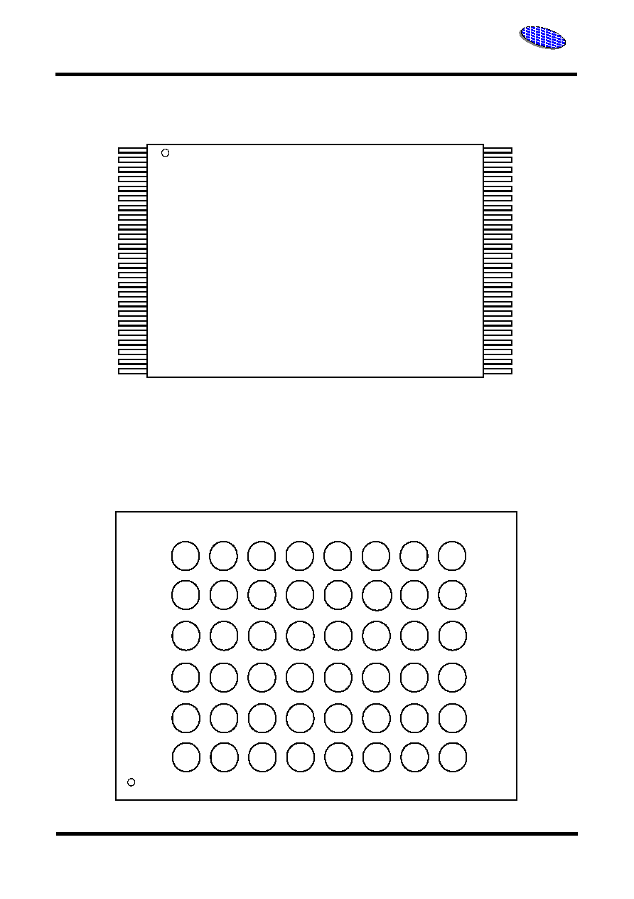
CONNECTION DIAGRAM
48-Ball FBGA (6 x 8 mm)
(Top View, Balls Facing Down)
A15
A14
A13
A12
A11
A10
A9
A8
A19
NC
WE#
RESET#
NC
NC
RY/BY#
A18
A17
A7
A6
A5
A4
A3
A2
A1
A16
BYTE#
Vss
DQ15/A-1
DQ7
DQ14
DQ6
DQ13
DQ5
DQ12
DQ4
Vcc
DQ11
DQ3
DQ10
DQ2
DQ9
DQ1
DQ8
DQ0
OE#
Vss
CE#
A0
1
2
3
4
5
6
7
8
9
10
11
12
13
14
15
16
17
18
19
20
21
22
23
24
48
47
46
45
44
43
42
41
40
39
38
37
36
35
34
33
32
31
30
29
28
27
26
25
48-Pin Standard TSOP
ES29LV160
A13
A12
A14
A15
A16
DQ15/
Vss
A9
WE#
OE#
CE#
A0
A1
A2
A4
NC
A11
DQ7
DQ14
DQ13
DQ6
NC
A19
A18
DQ5
NC
A5
DQ2
DQ0
DQ8
DQ9
DQ1
DQ10
DQ11
DQ3
DQ12
Vcc
DQ4
A3
A10
A B C D E F G H
6
5
4
3
2
1
BYTE#
A-1
A8
RESET#
RY/
A7
A17
A6
Vss
BY#