 | –≠–ª–µ–∫—Ç—Ä–æ–Ω–Ω—ã–π –∫–æ–º–ø–æ–Ω–µ–Ω—Ç: FS0101A | –°–∫–∞—á–∞—Ç—å:  PDF PDF  ZIP ZIP |
On-State Current
0.8 Amp
FS01...A/B
This series of Silicon Controlled R ectifiers
uses a high performance
PNPN technology.
This part is intended for general purpose
applications where high gate sensitivity is
required.
Jul - 02
Absolute Maximum Ratings, according to IEC publication No. 134
On-state Current
Average On-state Current
Non-repetitive On-State Current
Non-repetitive On-State Current
Fusing Current
Peak Reverse Gate Voltage
Peak Gate Current
Peak Gate Dissipation
Gate Dissipation
Operating Temperature
Storage Temperature
Soldering Temperature
I
T(RMS)
PARAMETER
CONDITIONS
Min.
Max.
Unit
Gate Trigger Current
< 200 µA
Off-State Voltage
200 V ˜ 600 V
SYMBOL
I
T(AV)
I
TSM
I
TSM
I
2
t
V
GRM
I
GM
P
GM
P
G(AV)
T
j
T
stg
T
sld
All Conduction Angle, T
L
= 55 ∫C
Half Cycle,
= 180 ∫, T
L
= 55 ∫C
Half Cycle, 60 Hz, T
j
= 25 ∫C
Half Cycle, 50 Hz, T
j
= 25∫ C
t
p
= 10ms, Half Cycle
I
GR
= 10 µA
20 µs max.
20 µs max.
20ms max.
1.6 mm from case, 10s max.
0.8
0.5
8
7
0.24
8
-40
-40
A
A
A
A
A
2
s
V
A
W
W
∫C
∫C
∫C
1
2
0.1
+125
+150
260
Repetitive Peak Off State
Voltage
PARAMETER
CONDITIONS
VOLTAGE
Unit
SYMBOL
V
DRM
V
RRM
R
GK
= 1 K
V
B
200
D
400
G
G
K
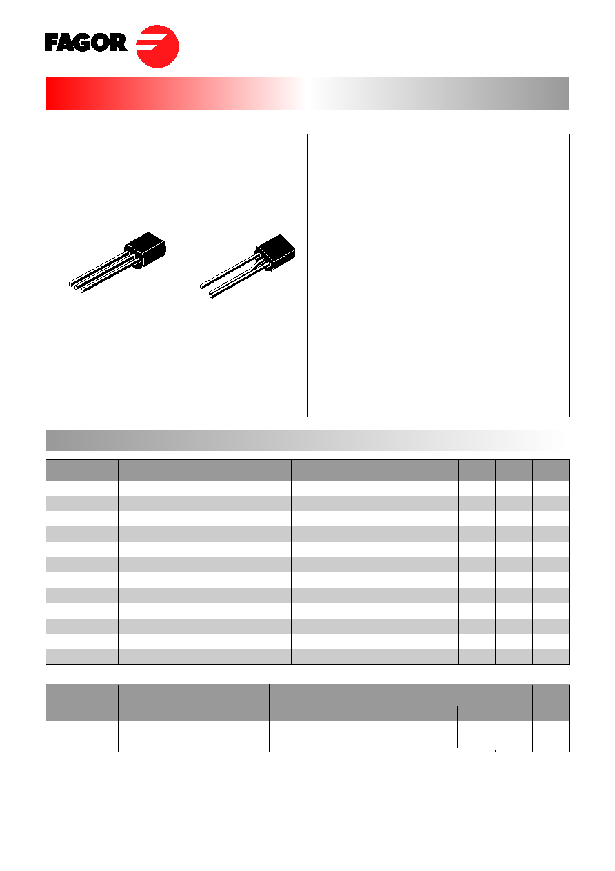
TO92
(Plastic)
RD26
(Plastic)
FS01...A
FS01...B
A
K
A
M
600
SENSITIVE GATE SCR
FS01...A/B
Jul - 02
Electrical Characteristics
Gate Trigger Current
Off-State Leakage Current
On-state Voltage
On-state Threshold Voltage
Dinamic Resistance
Gate Trigger Voltage
Gate Non Trigger Voltage
Holding Current
Latching Current
PARAMETER
CONDITIONS
SENSITIVITY
Unit
SYMBOL
I
GT
I
DRM
V
D
= 12 V
DC
, R
L
= 140
, T
j
= 25 ∫C
03
20
200
µA
04
15
50
100
1
1.95
0.95
600
0.8
0.1
80
µA
V
V
m
V
V
mA
mA
V/µs
MIN
MAX
MAX
MAX
MAX
MAX
MAX
MAX
MIN
MAX
MAX
MIN
MIN
50
80
150
A/µs
/ I
RRM
V
TM
V
T(O)
r
d
V
GT
I
H
I
L
dv / dt
di / dt
R
th(j-l)
R
th(j-a)
Critical Rate of Voltage
Rise
Critical Rate of Current Rise
Thermal Resistance
Junction-Leads for DC
Thermal Resistance
Junction-Ambient
∫C/W
∫C/W
V
D
= V
DRM
, R
GK
= 1K
,
T
j
= 125 ∫C
T
j
= 25 ∫C
V
R
= V
RRM
,
at I
T
= 1.6 Amp, tp = 380 µs, T
j
= 25 ∫C
T
j
= 125 ∫C
T
j
= 125 ∫C
V
D
= 12 V
DC
, R
L
= 140
, T
j
= 25 ∫C
I
T
= 50 mA
, R
GK
= 1K
, T
j
= 25 ∫C
I
G
= 1 mA
, R
GK
= 1K
, T
j
= 25 ∫C
V
D
= 0.67 x V
DRM
, R
GK
= 1K
,
T
j
= 125 ∫C
PART NUMBER INFORMATION
5
6
FAGOR
SCR
CURRENT
CASE
VOLTAGE
SENSITIVITY
F
S
01
01
B
A
00
FORMING
BU
PACKAGING
11
4
25
18
0.5
5
100
75
80
Tr
100 ns, F = 60 Hz,
T
j
= 125 ∫C
I
G
= 2 x I
GT
V
GD
V
D
= V
DRM
, R
L
= 3.3K
,
T
j
= 125 ∫C
R
GK
= 1K
,
SENSITIVE GATE SCR
01
1
20
02
200
75
75

Jul - 02
0
0.1
1
0.8
0.6
0.4
0.2
0
0.2 0.3 0.4
0.5 0.6 0.7 0.8
P (W)
IT(AV)(A)
= 30 ∫
= 60 ∫
= 90 ∫
= 120 ∫
= 180 ∫
DC
360 ∫
Fig. 1: Maximum average power dissipation
versus average on-state current
0
20
1
0.8
0.6
0.4
0.2
0
40
60
80
100 120 140
P (W)
Fig. 2: Correlation between maximum
average power dissipation and maximum
allowable temperature (Tamb and T lead).
T lead (∫C)
-45
-65
-85
-105
-125
Tamb (∫C)
Rth (j-a)
Rth (j-l)
1
0.8
0.6
0.4
0.2
0
I T(AV) (A)
Fig. 3: Average on-state current versus lead
temperature
0
20
40
60
80
100 120 140
DC
= 180 ∫
T lead (∫C)
10.0
9.0
8.0
7.0
6.0
5.0
4.0
3.0
2.0
1.0
0.0
Igt (Tj)
Fig. 5: Relative variation of gate trigger current
and holding current versus junction temperature.
-40 -20
0
60
80 100 120 140
Igt (Tj = 25 ∫C)
Ih (Tj)
Ih (Tj = 25 ∫C)
40
20
Ih
Tj (∫C)
Igt
1
10
100
1,000
Fig. 6: Non repetitive surge peak on-state
current versus number of cycles.
8
7
6
5
4
3
2
1
0
I TSM (A)
Tj initial = 25 ∫C
Number of cycles
1.00
0.10
0.01
Zth(j-a) / Rth(j-a)
Fig. 4: Relative variation of thermal impedance
junction to ambient versus pulse duration.
1E-3
1E-2
1E-1
1E+0
1E+1
1E+2 5E+2
tp (s)
FS01...A/B
SENSITIVE GATE SCR

Jul - 02
FS01...A/B
5.0
Ih(Rgk)
Fig. 9: Relative variation of holding
current versus gate-cathode resistance
(typical values).
1.0E+00
Ih(Rgk = 1k
)
1.0
0.1
Tj = 25 ∫C
Rgk (
)
1.0E+01 1.0E+02 1.0E+03 1.0E+04 1.0E+05 1.0E+06
0 0.5
10
1
0.1
1 1.5 2 2.5 3 3.5
Fig. 8: On-state characteristics (maximum
values).
ITM(A)
4 4.5 5 5.5
Tj max
Vto = 0.95 V
Rt = 0.600
VTM(V)
Tj max
Tj initial
25 ∫C
1
100
10
1
0.1
10
ITSM(A). I
2
t (A
2
s)
Fig. 7: Non repetitive surge peak on-state
current for a sinusoidal pulse with width:
tp
10 ms, and corresponding value of I
2
t.
Tj initial = 25 ∫C
tp(ms)
I
2
t
ITSM
PACKAGE MECHANICAL DATA
TO92 (Plastic)
A
B
C
D
E
F
G
H
a
b
REF.
DIMENSIONS
Milimeters
Min.
Typ.
Max.
Marking: type number
Weight: 0.2 g
PACKAGE MECHANICAL DATA
RD26 (Plastic)
-
4.55
2.42
1.15
4.55
12.7
3.55
-
0.38
0.33
1.5
4.6
2.54
1.27
4.6
14.1
3.6
1.5
0.43
0.38
-
4.65
2.66
1.39
4.65
15.5
3.65
-
0.48
0.43
A
B
C
D
E
F
G
a
b
REF.
DIMENSIONS
Millimeters
Min.
Typ.
Max.
-
4.55
2.42
1.15
4.55
12.7
3.55
0.38
0.33
1.5
4.6
2.54
1.27
4.6
14.1
3.6
0.43
0.38
-
4.65
2.66
1.39
4.65
15.5
3.65
0.48
0.43
Marking: type number
Weight: 0.2 g
A
B
C
D
G
b
E
F
H
a
C
D
G
A
a
B
E
F
45∫
b
SENSITIVE GATE SCR