 | –≠–ª–µ–∫—Ç—Ä–æ–Ω–Ω—ã–π –∫–æ–º–ø–æ–Ω–µ–Ω—Ç: FS0101N | –°–∫–∞—á–∞—Ç—å:  PDF PDF  ZIP ZIP |

On-State Current
0.8 Amp
FS01...N
These series of Silicon Controlled
R ectifiers uses a high performance
PNPN technology.
These parts are intended for general
purpose applications where high gate
sensitivity is required using surface mount
technology.
Absolute Maximum Ratings, according to IEC publication No. 134
On-state Current
Average On-state Current
Non-repetitive On-State Current
Non-repetitive On-State Current
Fusing Current
Peak Reverse Gate Voltage
Peak Gate Current
Peak Gate Dissipation
Gate Dissipation
Operating Temperature
Storage Temperature
Soldering Temperature
I
T(RMS)
PARAMETER
CONDITIONS
Min.
Max.
Unit
SOT223
(Plastic)
Gate Trigger Current
< 200 µA
Off-State Voltage
200 V ˜ 600 V
SYMBOL
I
T(AV)
I
TSM
I
TSM
I
2
t
V
GRM
I
GM
P
GM
P
G(AV)
T
j
T
stg
T
sld
All Conduction Angle, T
tab
= 70 ∫C
Half Cycle,
= 180 ∫, T
tab
= 70 ∫C
Half Cycle, 60 Hz, T
j
= 25 ∫C
Half Cycle, 50 Hz, T
j
= 25 ∫C
t
p
= 10ms, Half Cycle
I
GR
= 10 µA
20 µs max.
20 µs max.
20ms max.
1.6 mm from case, 10s max.
0.8
0.5
8
7
0.24
8
-40
-40
A
A
A
A
A
2
s
V
A
W
W
∫C
∫C
∫C
1
2
0.1
+125
+150
260
Jul - 02
Repetitive Peak Off State
Voltage
PARAMETER
CONDITIONS
VOLTAGE
Unit
SYMBOL
V
DRM
V
RRM
R
GK
= 1 K
V
B
200
D
400
M
600
SURFACE MOUNT SCR

Jul - 02
PART NUMBER INFORMATION
FAGOR
SCR
CURRENT
CASE
VOLTAGE
SENSITIVITY
F
S
01
01
B
N
00
FORMING
RB
PACKAGING
FS01...N
SURFACE MOUNT SCR
Electrical Characteristics
Gate Trigger Current
Off-State Leakage Current
On-state Voltage
On-state Threshold Voltage
Dinamic Resistance
Gate Trigger Voltage
Gate Non Trigger Voltage
Holding Current
Latching Current
PARAMETER
CONDITIONS
SENSITIVITY
Unit
SYMBOL
I
GT
I
DRM
V
D
= 12 V
DC
, R
L
= 140
, T
j
= 25 ∫C
03
20
200
µA
04
15
50
100
1
1.95
0.95
600
0.8
0.1
80
µA
V
V
m
V
V
mA
mA
V/µs
MIN
MAX
MAX
MAX
MAX
MAX
MAX
MAX
MIN
MAX
MAX
MIN
MIN
50
80
150
A/µs
/ I
RRM
V
TM
V
T(O)
r
d
V
GT
I
H
I
L
dv / dt
di / dt
R
th(j-l)
R
th(j-a)
Critical Rate of Voltage
Rise
Critical Rate of Current Rise
Thermal Resistance
Junction-Leads for DC
Thermal Resistance
Junction-Ambient
∫C/W
∫C/W
V
D
= V
DRM
, R
GK
= 1K
,
T
j
= 125 ∫C
T
j
= 25 ∫C
V
R
= V
RRM
,
at I
T
= 1.6 Amp, tp = 380 µs, T
j
= 25 ∫C
T
j
= 125 ∫C
T
j
= 125 ∫C
V
D
= 12 V
DC
, R
L
= 140
, T
j
= 25 ∫C
I
T
= 50 mA
, R
GK
= 1K
, T
j
= 25 ∫C
I
G
= 1 mA
, R
GK
= 1K
, T
j
= 25 ∫C
V
D
= 0.67 x V
DRM
, R
GK
= 1K
,
T
j
= 125 ∫C
5
6
11
4
25
18
0.5
5
100
75
80
Tr
100 ns, F = 60 Hz,
T
j
= 125 ∫C
I
G
= 2 x I
GT
V
GD
V
D
= V
DRM
, R
L
= 3.3K
,
T
j
= 125 ∫C
R
GK
= 1K
,
01
1
20
02
200
75
75
FS01...N
0
0.1
1
0.8
0.6
0.4
0.2
0
0.2 0.3 0.4
0.5 0.6 0.7 0.8
P (W)
IT(AV)(A)
= 30 ∫
= 60 ∫
= 90 ∫
= 120 ∫
= 180 ∫
DC
360 ∫
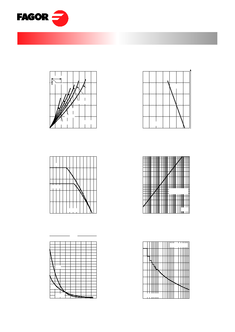
Fig. 1: Maximum average power dissipation
versus average on-state current
0
20
1
0.8
0.6
0.4
0.2
0
40
60
80
100 120 140
P (W)
Fig. 2: Correlation between maximum
average power dissipation and maximum
allowable temperature (Tamb and T tab).
T tab (∫C)
-95
-100
-105
-110
-115
-120
-125
Tamb (∫C)
Rth (j-a)
1
0.8
0.6
0.4
0.2
0
I T(AV) (A)
Fig. 3: Average on-state current versus tab
temperature
0
20
40
60
80
100 120 140
DC
= 180 ∫
T
tab
(∫C)
10.0
9.0
8.0
7.0
6.0
5.0
4.0
3.0
2.0
1.0
0.0
Igt (Tj)
Fig. 5: Relative variation of gate trigger current
and holding current versus junction temperature.
-40 -20
0
60
80 100 120 140
Igt (Tj = 25 ∫C)
Ih (Tj)
Ih (Tj = 25 ∫C)
40
20
Ih
Tj (∫C)
Igt
1
10
100
1,000
Fig. 6: Non repetitive surge peak on-state
current versus number of cycles.
8
7
6
5
4
3
2
1
0
I TSM (A)
Tj initial = 25 ∫C
Number of cycles
1.00
0.10
0.01
Zth(j-a) / Rth(j-a)
Fig. 4: Relative variation of thermal impedance
junction to ambient versus pulse duration.
1E-3
1E-2
1E-1
1E+0
1E+1
1E+2 5E+2
tp (s)
Standard foot print,
e (Cu) = 35 µm
Jul - 02
SURFACE MOUNT SCR

FS01...N
1
100
10
1
0.1
10
ITSM(A). I
2
t (A
2
s)
Fig. 7: Non repetitive surge peak on-state
current for a sinusoidal pulse with width:
tp
10 ms, and corresponding value of I
2
t.
0 0.5
10
1
0.1
1 1.5 2 2.5 3 3.5
Fig. 8: On-state characteristics (maximum
values).
5.0
Ih(Rgk)
Fig. 9: Relative variation of holding
current versus gate-cathode resistance
(typical values).
1.0E+00
Tj initial = 25 ∫C
tp(ms)
I
2
t
ITSM
ITM(A)
4 4.5 5 5.5
Tj max
Vto = 0.95 V
Rt = 0.600
VTM(V)
Tj max
Tj initial
25 ∫C
Ih(Rgk = 1k
)
1.0
0.1
Tj = 25 ∫C
Rgk (
)
1.0E+01 1.0E+02 1.0E+03 1.0E+04 1.0E+05 1.0E+06
Jul - 02
PACKAGE MECHANICAL DATA
SOT223 (Plastic)
A
B
C
D
E
F
G
H
I
J
K
REF.
DIMENSIONS
Milimeters
Min.
Typ.
Max.
Weight: 0.11 g
FOOT PRINT
6.30
6.70
3.30
-
-
2.95
0.65
1.50
0.50
-
0.25
6.50
7.00
3.50
4.60
2.30
3.00
0.70
1.60
0.60
0.02
0.30
6.70
7.30
3.70
-
-
3.15
0.85
1.70
0.70
0.05
0.35
3.3
1.5
1.5
(3x) 1
2.3
4.6
6.4
G
F
A
16∫ max. (4x)
H
D
E
I
B
C
J
10∫ max.
K
SURFACE MOUNT SCR