 | –≠–ª–µ–∫—Ç—Ä–æ–Ω–Ω—ã–π –∫–æ–º–ø–æ–Ω–µ–Ω—Ç: FS0401I | –°–∫–∞—á–∞—Ç—å:  PDF PDF  ZIP ZIP |
On-State Current
4 Amp
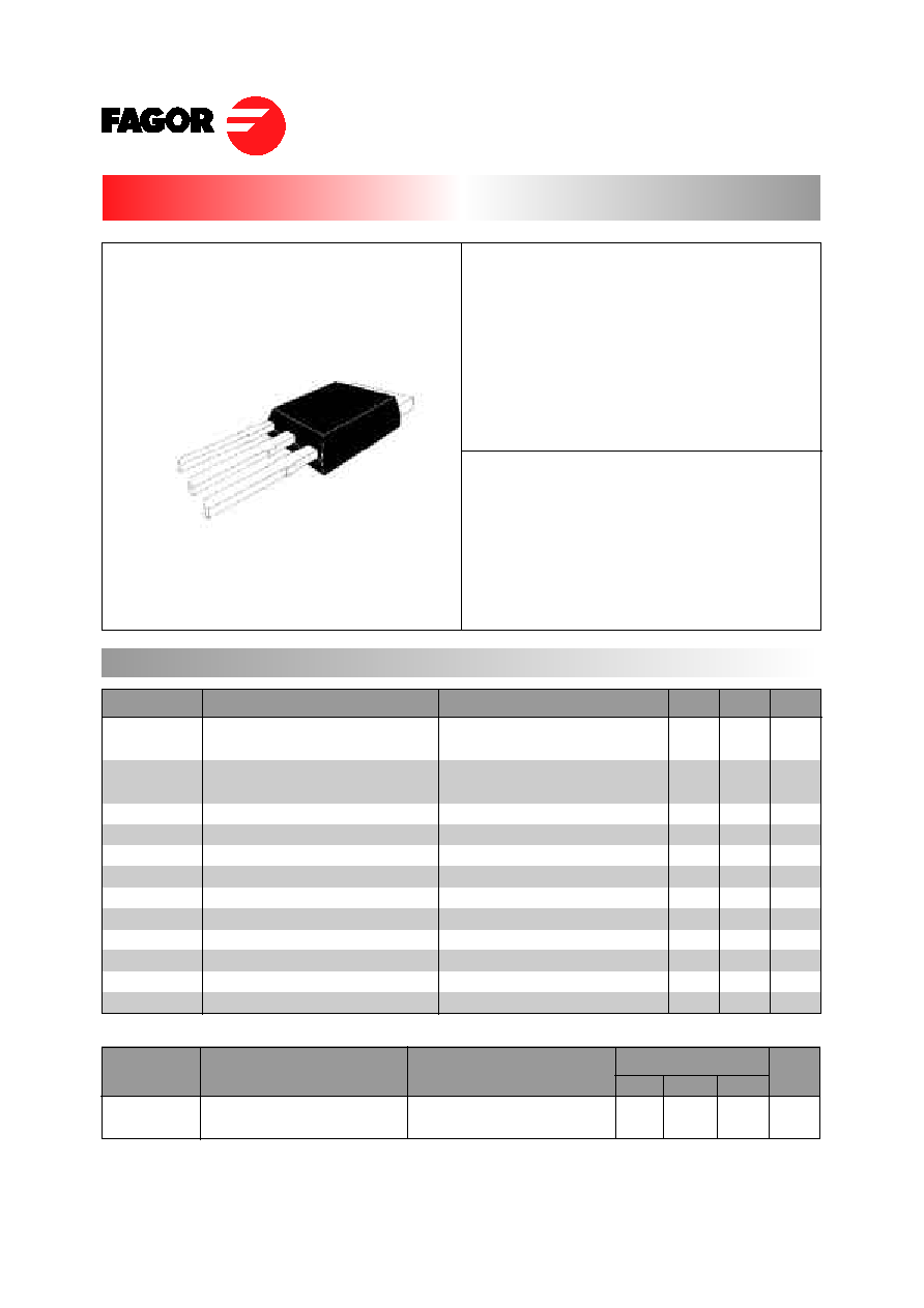
FS04...I
SENSITIVE GATE SCR
These series of Silicon Controlled R ectifier use
a high performance PNPN technology.
These parts are intended for general purpose
applications where high gate sensitivity is
required like small engine ignition, SMPS
crowbar protection, food procesor.
Absolute Maximum Ratings, according to IEC publication No. 134
On-state Current
Average On-state Current
Non-repetitive On-State Current
Non-repetitive On-State Current
Fusing Current
Peak Reverse Gate Voltage
Peak Gate Current
Peak Gate Dissipation
Gate Dissipation
Operating Temperature
Storage Temperature
Lead Temperature for Soldering
I
T(RMS)
PARAMETER
CONDITIONS
Min.
Max.
Unit
IPAK
(Plastic)
Gate Trigger Current
< 200 µA
Off-State Voltage
200 V ˜ 600 V
SYMBOL
I
T(AV)
I
TSM
I
TSM
I
2
t
V
GRM
I
GM
P
GM
P
G(AV)
T
j
T
stg
T
L
180∫ Conduction Angle, Tc = 105 ∫C
Ta = 25 ∫C
Half Cycle,
= 180 ∫, Tc = 105 ∫C
Ta = 25 ∫C
Half Cycle, 60 Hz
Half Cycle, 50 Hz
t = 10ms, Half Cycle
I
GR
= 10 µA
20 µs max.
20 µs max.
20 ms max.
10s at 4.5mm from case
4
1.35
2.5
0.9
33
30
4.5
8
-40
-40
A
A
A
A
A
2
s
V
A
W
W
∫C
∫C
∫C
1.2
3
0.2
+125
+150
260
Jun - 02
K
A
G
A
Repetitive Peak Off State
Voltage
PARAMETER
CONDITIONS
VOLTAGE
Unit
SYMBOL
V
DRM
V
RRM
R
GK
= 1 K
B
200
V
D
400
M
600
FS04...I
SENSITIVE GATE SCR
Electrical Characteristics
Gate Trigger Current
Off-State Leakage Current
On-state Voltage
Gate Trigger Voltage
Gate Non Trigger Voltage
Holding Current
Latching Current
PARAMETER
CONDITIONS
SENSITIVITY
Unit
SYMBOL
I
GT
I
DRM
V
D
= 12 V
DC
, R
L
= 33
, T
j
= 25 ∫C
01
1
20
µA
04
15
50
02
200
03
20
200
1
5
1.6
0.8
0.1
5
6
10
10
5
10
mA
µA
V
V
V
mA
mA
V/µs
MIN
MAX
MAX
MAX
MAX
MAX
MIN
MAX
MAX
MIN
MIN
50
7.5
100
A/µs
/ I
RRM
V
TM
V
GT
I
H
I
L
dv / dt
di / dt
Critical Rate of Voltage
Rise
Critical Rate of Current Rise
V
D
= V
DRM
, R
GK
= 220
, T
j
= 125 ∫C
T
j
= 25 ∫C
V
R
= V
RRM
,
at I
T
= 8 Amp, tp = 380 µs, T
j
= 25 ∫C
V
D
= 12 V
DC
, R
L
= 33
, T
j
= 25 ∫C
I
T
= 50 mA
, R
GK
= 1K
, T
j
= 25 ∫C
I
G
= 1 mA
, R
GK
= 1K
, T
j
= 25 ∫C
V
D
= 0.67 x V
DRM
, R
GK
= 220
,
T
j
= 125 ∫C
PART NUMBER INFORMATION
Jun - 02
∫C/W
R
th(j-a)
Thermal Resistance
Junction-Ambient
∫C/W
R
th(j-c)
Thermal Resistance
Junction-Case for DC
FAGOR
SCR
CURRENT
CASE
VOLTAGE
SENSITIVITY
F
S
04
01
B
I
00
FORMING
TU
PACKAGING
Tr
100 ns, F = 60 Hz,
T
j
= 125 ∫C
I
G
= 2 x I
GT
V
GD
V
D
= V
DRM
, R
L
= 3.3K
,
T
j
= 125 ∫C
R
GK
= 220
,
FS04...I
SENSITIVE GATE SCR
0
5
4
3
2
1
0
0.5
1
1.5
2
P (W)
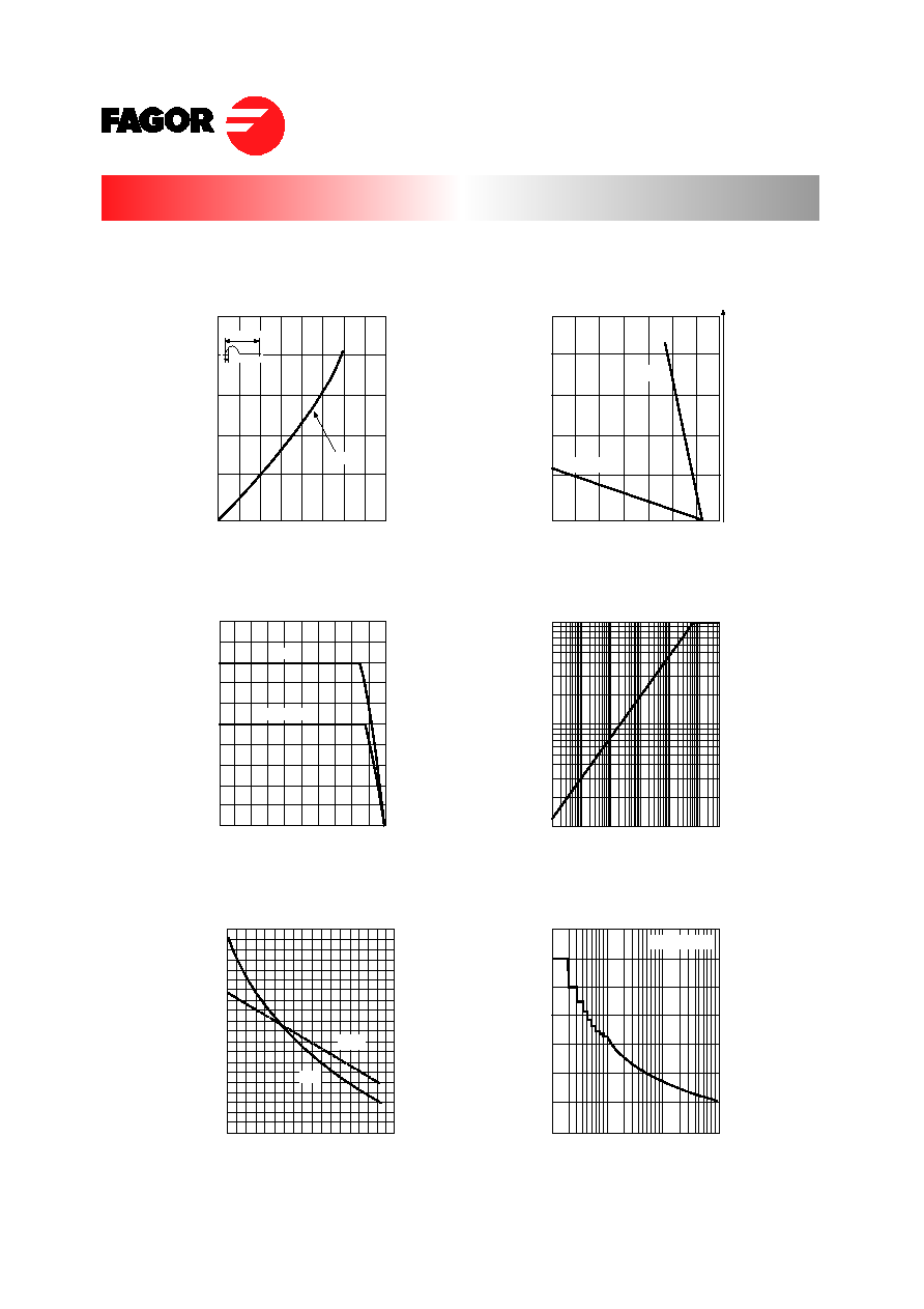
Fig. 1: Maximum average power dissipation
versus average on-state current
0
20
5
4
3
2
1
0
40
60
80
100 120 140
P (W)
Fig. 2: Correlation between maximum
average power dissipation and maximum
allowable temperature (Tamb and T case).
T case (∫C)
85
95
105
115
125
Fig. 3: Average on-state current versus case
temperature
Fig. 5: Relative variation of gate trigger current
and holding current versus junction temperature.
1
10
100
1000
Fig. 6: Non repetitive surge peak on-state
current versus number of cycles.
35
30
25
20
15
10
5
0
I TSM (A)
Tj initial = 25 ∫C
1.00
0.10
0.01
Zth(j-a) / Rth(j-a)
Fig. 4: Relative variation of thermal impedance
junction to ambient versus pulse duration.
1E-3
1E-2
1E-1
1E+0
1E+1
1E+2 5E+2
Jun- 02
Rth (j-a)
2.5
3
3.5
Tamb (∫C)
Number of cycles
tp (s)
IT(AV)(A)
4
360 ∫
Rth (j-c)
= 80 ∫
I T(av) (A)
T case (∫C)
5
4
3
2
1
0
0
25
50
75
100
125
= 180 ∫
D.C.
IGT, IH (Tj) / IGT, IH (Tj = 25 ∫C)
Tj (∫C)
2.0
1.8
1.6
1.4
1.2
1.0
0.8
0.6
0.4
0.2
0.0
-40 -20
20
60
80 100
0
40
120 140
IH & IL
IGT
FS04...I
Jun - 02
SENSITIVE GATE SCR
ITSM(A). I
2
t (A
2
s)
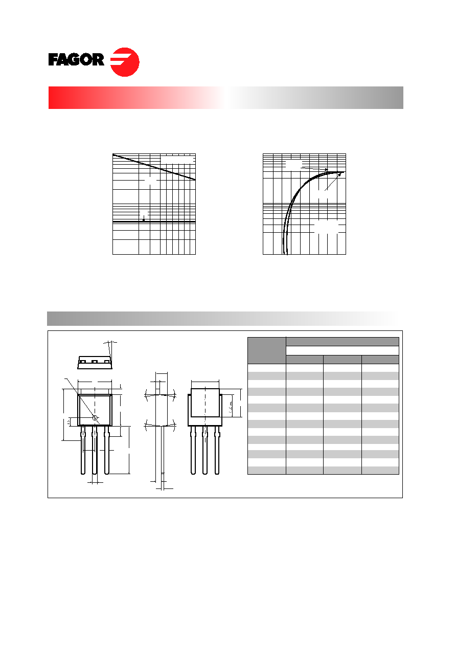
Fig. 7: Non repetitive surge peak on-state
current for a sinusoidal pulse with width:
tp
10 ms, and corresponding value of I
2
t.
100
10
1
1
10
Tj initial = 25 ∫C
tp(ms)
ITSM
I
2
t
Fig. 8: On-state characteristics (maximum
values).
100
10
1
ITM(A)
0
0.5 1 1.5
2 2.5
3 3.5 4 4.5
Tj max
Tj initial
25 ∫C
VTM(V)
Tj max
Vto = 0.95 V
Rt = 0.100
PACKAGE MECHANICAL DATA
IPAK TO 251-AA
Marking: type number
Weight: 0.2 g
¯1x0.15
E
D
L3
L1
L
b
e
b1
H
8∫
±2∫
A
8∫
±2∫
8∫
±2∫
8∫
±2∫
c2
c
A1
D1
E1
8∫
±2∫
A
A1
b
b1
c
c2
D
D1
E
E1
e
L
L1
L3
REF.
DIMENSIONS
Milimeters
Min.
Nominal
Max.
2.19
0.89
0.64
0.76
0.46
5.97
5.21
6.35
5.21
8.89
1.91
0.89
2.3±0.08
1.067±0.01
0.75±0.1
0.95
0.8±0.013
6.1±0.1
6.58±0.14
5.36±0.1
2.28BSC
9.2±0.2
2±0.1
2.38
1.14
0.89
1.14
0.58
6.22
5.52
6.73
5.46
9.65
2.28
1.27