 | –≠–ª–µ–∫—Ç—Ä–æ–Ω–Ω—ã–π –∫–æ–º–ø–æ–Ω–µ–Ω—Ç: FT0102DN | –°–∫–∞—á–∞—Ç—å:  PDF PDF  ZIP ZIP |

SOT223
(Plastic)
On-State Current
1 Amp
FT01...N
The FT01 series of TRIACs uses a high
performance PNPN technology.
These parts are intended for general
purpose applications where logic
compatible gate sensitivity is required
using surface mount technology.
Mar - 03
Gate Trigger Current
< 3 mA to < 25 mA
Off-State Voltage
200 V ˜ 400 V (02, 03)
200 V ˜ 600 V (04, 05, 07, 09, 10)
MT1
MT2
MT2
G
SURFACE MOUNT TRIAC
Repetitive Peak Off State
Voltage
PARAMETER
VOLTAGE
Unit
SYMBOL
V
DRM
V
RRM
B
200
V
M *
600
D
400
* 04, 05, 07, 09 & 10 sensitivities
Absolute Maximum Ratings, according to IEC publication No. 134
RMS On-state Current
Non-repetitive On-State Current
Non-repetitive On-State Current
Fusing Current
Peak Gate Current
Peak Gate Dissipation
Gate Dissipation
Critical rate of rise of on-state current
Operating Temperature
Storage Temperature
Soldering Temperature
I
T(RMS)
PARAMETER
CONDITIONS
Min.
Max.
Unit
SYMBOL
I
TSM
I
TSM
I
2
t
I
GM
P
GM
P
G(AV)
T
j
T
stg
T
sld
All Conduction Angle, T
ab
= 90 ∫C
Half Cycle, 60 Hz
Half Cycle, 50 Hz
t
p
= 10 ms, Half Cycle
20 µs max.
20 µs max.
20 ms max.
1.6 mm from case, 10s max.
-40
-40
A
A
A
A
2
s
A
W
W
A/µs
∫C
∫C
∫C
1.0
8.5
8
0.35
1
2
0.1
20
+125
+150
260
di/dt
Tr
100 ns, F = 120 Hz
T
j
= 125 ∫C
I
G
= 2 x I
GT

Mar - 03
PART NUMBER INFORMATION
FAGOR
TRIAC
CURRENT
CASE
VOLTAGE
SENSITIVITY
F
T
01
05
B
N
00
FORMING
RB
PACKAGING
FT01...N
SURFACE MOUNT TRIAC
Electrical Characteristics
Gate Trigger Current
Off-State Leakage Current
Threshold Voltage
Dynamic Resistance
On-state Voltage
Gate Trigger Voltage
Gate Non Trigger Voltage
Holding Current
Latching Current
Critical Rate of Voltage Rise
PARAMETER
CONDITIONS
SENSITIVITY
Unit
SYMBOL
I
GT
I
DRM
V
D
= 12 V
DC
, R
L
= 30
, T
j
= 25 ∫C
mA
0.5
5
0.95
400
1.5
1.3
0.2
10
10
20
20
1
60
150
mA
µA
V
m
V
V
V
mA
mA
V/µs
V/µs
MAX
MAX
MAX
MAX
MAX
MAX
MAX
MAX
MIN
MAX
MAX
MAX
MIN
MIN
/I
RRM
V
TM
*
V
GT
V
GD
I
H
*
I
L
dv / dt*
R
th(j-a)
Thermal Resistance
Junction-Ambient
V
D
= V
DRM
,
T
j
= 125 ∫C
T
j
= 25 ∫C
V
R
= V
RRM
,
I
T
= 1.1 Amp, tp = 380 µs, T
j
= 25 ∫C
V
D
= 12 V
DC
, R
L
= 30
, T
j
= 25 ∫C
I
T
= 50 mA
T
j
= 25 ∫C
I
G
= 1.2 I
GT
,
T
j
= 25 ∫C
V
D
= 0.67 x V
DRM
, Gate open
T
j
= 125 ∫C
Quadrant
Q1˜Q3
Q4
Q1˜Q4
Q1˜Q4
Q1,Q3,Q4
Q2
V
D
= V
DRM
, R
L
= 3.3K
, T
j
= 125 ∫C
∫C/W
∫C/W
(*) For either polarity of electrode MT2 voltage with reference to electrode MT1.
R
th(j-l)
Thermal Resistance
Junction-Leads for AC
(dv/dt)c*
(di/dt)c= 0.44 A/ms T
j
= 110 ∫C
V
to
R
d
T
j
= 125 ∫C
T
j
= 125 ∫C
07
5
7
05
5
5
03
3
5
02
3
3
09
10
10
7
7
14
10
0.5
25
25
50
2
04
5
Critidal rise rate of
commutating off-state
Voltage
10
25
25
25
50
200
4.4

Mar - 03
Fig. 1: Maximum power dissipation versus
RMS on-state current
0
20
1.6
1.4
1.2
1.0
0.8
0.6
0.4
0.2
0.0
40
60
80
100 120 140
P (W)
Fig. 2: Correlation between maximum
power dissipation and maximum allowable
temperature (Tamb and T tab).
T tab (∫C)
-90
-95
-100
-105
-110
-115
-120
-125
Rth (j-a) ∫C/W
Fig. 3: RMS on-state current versus tab
temperature
2.6
2.4
2.2
2.0
1.8
1.6
1.4
1.2
1.0
0.8
0.6
0.4
Igt (Tj)
Fig. 5: Relative variation of gate trigger current
and holding current versus junction temperature.
-40 -20
0
60
80 100 120 140
Igt (Tj = 25 ∫C)
Ih (Tj)
Ih (Tj = 25 ∫C)
40
20
1
10
100
1000
Fig. 6: Non repetitive surge peak on-state
current versus number of cycles.
8
6
4
2
0
I TSM (A)
Tj initial = 25 ∫C
1.00
0.10
0.01
Zth(j-a) / Rth(j-a)
Fig. 4: Relative variation of thermal impedance
junction to ambient versus pulse duration.
1E-3
1E-2
1E-1
1E+0
1E+1
1E+2 5E+2
1.2
1.0
0.8
0.6
0.4
0.2
0
I T(RMS) (A)
0
20
40
60
80
100
120
= 180 ∫
10
30
50
70
90
110
130
Igt
Ih
0.0 0.1
1.6
1.4
1.2
1.0
0.8
0.6
0.4
0.2
0.0
0.2 0.3 0.4 0.5 0.6 0.7 0.8
P (W)
Rth (j-l) ∫C/W
Standard foot print, e(Cu) = 35 µm
180 ∫
0.9 1.0
= 180 ∫
= 120 ∫
= 90 ∫
= 60 ∫
= 30 ∫
Tamb (∫C)
Tj (∫C)
Number of cycles
tp (s)
T tab (∫C)
IT(RMS)(A)
FT01...N
SURFACE MOUNT TRIAC
Mar - 03
0 0.5
10
1
0.1
1 1.5 2 2.5 3 3.5
Fig. 8: On-state characteristics (maximum
values).
ITM(A)
4
1
100
10
1
0.1
10
ITSM(A). I
2
t (A
2
s)
Fig. 7: Non repetitive surge peak on-state
current for a sinusoidal pulse with width:
tp
10 ms, and corresponding value of I
2
t.
Tj initial = 25 ∫C
tp(ms)
I
2
t
ITSM
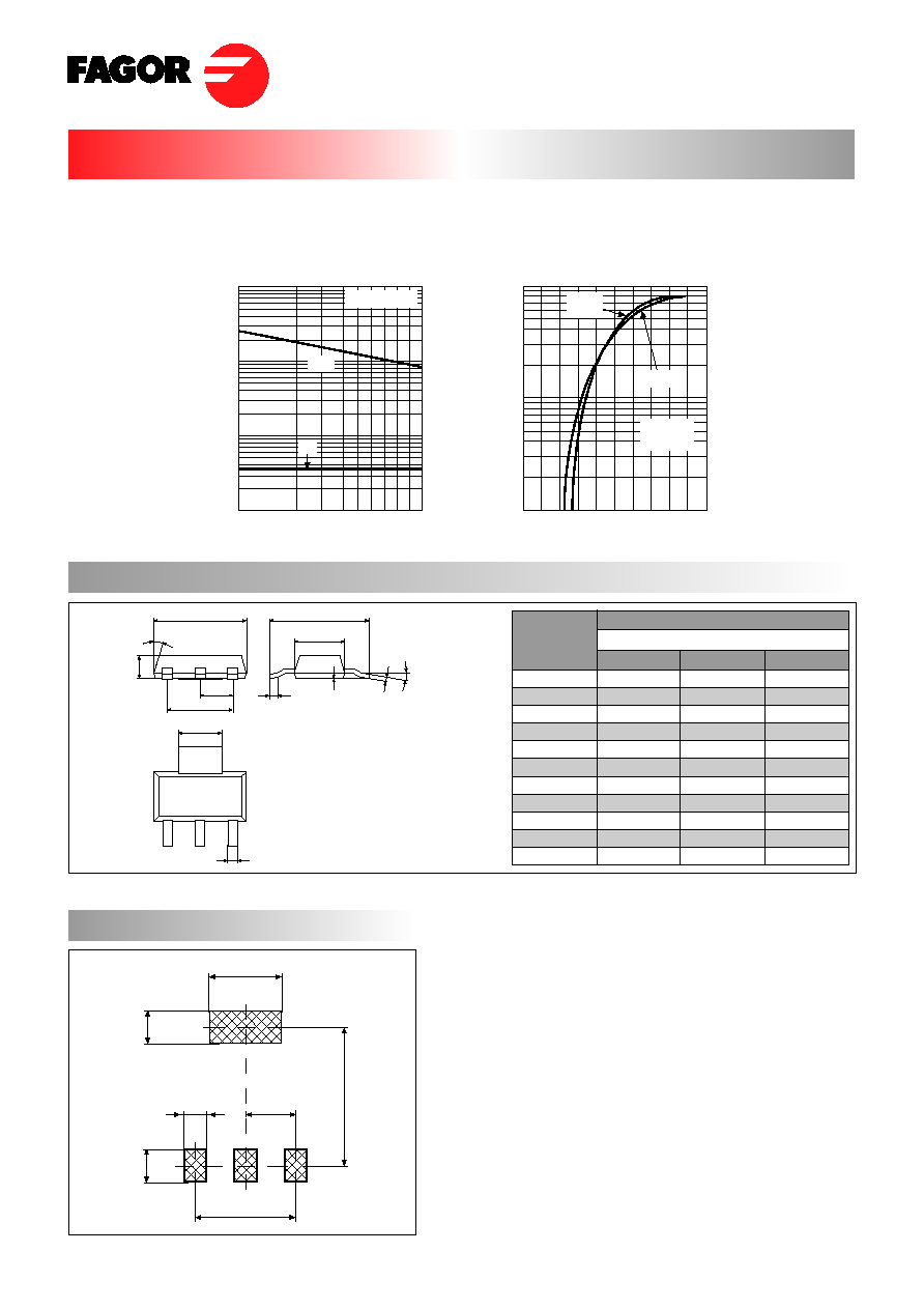
PACKAGE MECHANICAL DATA
SOT223 (Plastic)
A
B
C
D
E
F
G
H
I
J
K
REF.
DIMENSIONS
Milimeters
Min.
Typ.
Max.
Weight: 0.11 g
FOOT PRINT
6.30
6.70
3.30
-
-
2.95
0.65
1.50
0.50
-
0.25
6.50
7.00
3.50
4.60
2.30
3.00
0.70
1.60
0.60
0.02
0.30
6.70
7.30
3.70
-
-
3.15
0.85
1.70
0.70
0.05
0.35
3.3
1.5
1.5
(3x) 1
2.3
4.6
6.4
G
F
A
16∫ max. (4x)
H
D
E
I
B
C
J
10∫ max.
K
4.5 5
Tj max
Vto = 1.10 V
Rt = 0.420
VTM(V)
Tj max
Tj initial
25 ∫C
FT01...N
SURFACE MOUNT TRIAC