 | –≠–ª–µ–∫—Ç—Ä–æ–Ω–Ω—ã–π –∫–æ–º–ø–æ–Ω–µ–Ω—Ç: 100310QI | –°–∫–∞—á–∞—Ç—å:  PDF PDF  ZIP ZIP |
© 1999 Fairchild Semiconductor Corporation
DS010943
www.fairchildsemi.com
October 1991
Revised November 1999
1
00310 Low
Skew
2
:
8 Dif
f
er
enti
al Clo
ck
Dr
iver
100310
Low Skew 2:8 Differential Clock Driver
General Description
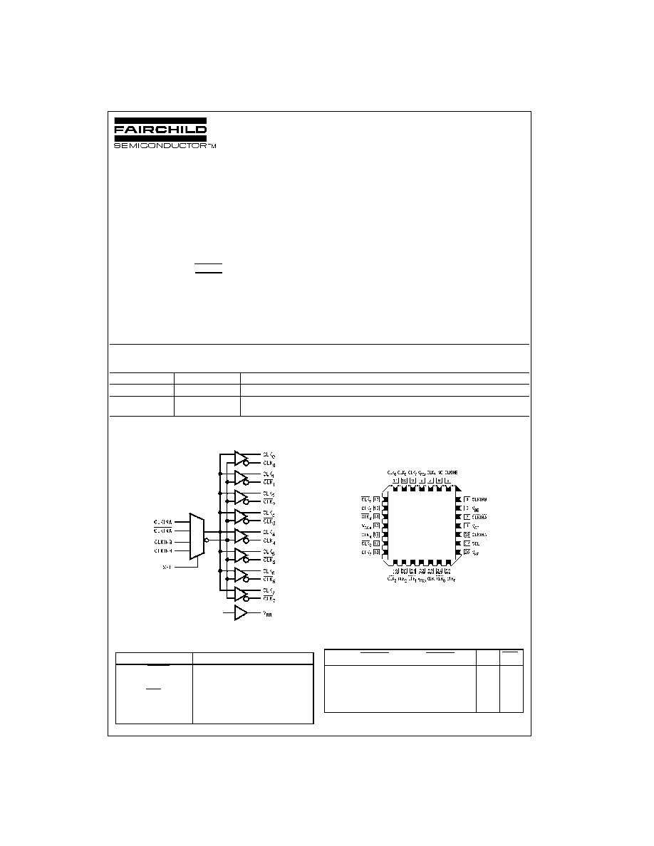
The 100310 is a low skew 8-bit differential clock driver
which is designed to select between two separate differen-
tial clock inputs. The low output to output skew (
<
50 ps) is
maintained for either clock input. A LOW on the select pin
(SEL) selects CLKINA, CLKINA and a HIGH on the SEL
pin selects the CLKINB, CLKINB inputs.
The 100310 is ideal for those applications that need the
ability to freely select between two clocks, or to maintain
the ability to switch to an alternate or backup clock should a
problem arise with the primary clock source.
A V
BB
output is provided for single-ended operation.
Features
s
Low output to output skew
s
Differential inputs and outputs
s
Allows multiplexing between two clock inputs
s
Voltage compensated operating range:
-
4.2V to
-
5.7V
s
Available to industrial grade temperature range
(PLCC package only)
Ordering Code:
Devices also available in Tape and Reel. Specify by appending the suffix letter "X" to the ordering code.
Logic Symbol
Pin Descriptions
Connection Diagram
28-Pin PLCC
Truth Table
Order Number
Package Number
Package Description
100310QC
V28A
28-Lead Plastic Lead Chip Carrier (PLCC), JEDEC MO-047, 0.450 Square
100310QI
V28A
28-Lead Plastic Lead Chip Carrier (PLCC), JEDEC MO-047, 0.450 Square
Industrial Temperature Range (
-
40
∞
C to
+
85
∞
C)
Pin Names
Description
CLKIN
n
, CLKIN
n
Differential Clock Inputs
SEL
Select
CLK
0≠7
, CLK
0≠8
Differential Clock Outputs
V
BB
V
BB
Output
NC
No Connect
CLKINA CLKINA CLKINB CLKINB SEL CLK
n
CLK
n
H
L
X
X
L
H
L
L
H
X
X
L
L
H
X
X
H
L
H
H
L
X
X
L
H
H
L
H
www.fairchildsemi.com
2
100310
Absolute Maximum Ratings
(Note 1)
Recommended Operating
Conditions
Note 1: The "Absolute Maximum Ratings" are those values beyond which
the safety of the device cannot be guaranteed. The device should not be
operated at these limits. The parametric values defined in the Electrical
Characteristics tables are not guaranteed at the absolute maximum rating.
The "Recommended Operating Conditions" table will define the conditions
for actual device operation.
Note 2: ESD testing conforms to MIL-STD-883, Method 3015.
Commercial Version
DC Electrical Characteristics
(Note 3)
V
EE
=
-
4.2V to
-
5.7V, V
CC
=
V
CCA
=
GND, T
C
=
0
∞
C to
+
85
∞
C
Note 3: The specified limits represent the "worst case" value for the parameter. Since these values normally occur at the temperature extremes, additional
noise immunity and guardbanding can be achieved by decreasing the allowable system operating ranges. Conditions for testing shown in the tables are cho-
sen to guarantee operation under "worst case" conditions.
Storage Temperature (T
STG
)
-
65
∞
C to
+
150
∞
C
Maximum Junction Temperature (T
J
)
+
150
∞
C
Pin Potential to Ground Pin (V
EE
)
-
7.0V to
+
0.5V
Input Voltage (DC)
V
EE
to
+
0.5V
Output Current (DC Output HIGH)
-
50 mA
ESD (Note 2)
2000V
Case Temperature (T
C
)
Commercial
0
∞
C to
+
85
∞
C
Industrial
-
40
∞
C to
+
85
∞
C
Supply Voltage (V
EE
)
-
5.7V to
-
4.2V
Symbol
Parameter
Min
Typ
Max
Units
Conditions
V
OH
Output HIGH Voltage
-
1025
-
955
-
870
mV
V
IN
=
V
IH
(Max)
Loading with
V
OL
Output LOW Voltage
-
1830
-
1705
-
1620
mV
or V
IL
(Min)
50
to
-
2.0V
V
OHC
Output HIGH Voltage
-
1035
mV
V
IN
=
V
IH
Loading
with
V
OLC
Output LOW Voltage
-
1610
mV
or V
IL
(Max)
50
to
-
2.0V
V
BB
Output Reference Voltage
-
1380
-
1320
-
1260
mV
I
VBB
=
-
250
µ
A
V
DIFF
Input Voltage Differential
150
mV
Required for Full Output Swing
V
CM
Common Mode Voltage
V
CC
-
2.0
V
CC
-
0.5
V
V
IH
Input HIGH Voltage
-
1165
-
870
mV
Guaranteed HIGH Signal for All Inputs
V
IL
Input LOW Voltage
-
1830
-
1475
mV
Guaranteed LOW Signal for All Inputs
I
IL
Input LOW Current
0.50
µ
A
V
IN
=
V
IL
(Min)
I
IH
Input HIGH Current
240
µ
A
V
IN
=
V
IH
(Max)
I
CBO
Input Leakage Current
-
10
µ
A
V
IN
=
V
EE
I
EE
Power Supply Current
-
100
-
40
mA
Inputs Open

3
www.fairchildsemi.com
1
00310
Commercial Version
(Continued)
AC Electrical Characteristics
V
EE
=
-
4.2V to
-
5.7V, V
CC
=
V
CCA
=
GND
Note 4: t
PS
describes opposite edge skews, i.e. the difference between the delay of a differential output signal pair's LOW-to-HIGH and HIGH-to-LOW prop-
agation delays. With differential signal pairs, a LOW-to-HIGH or HIGH-to-LOW transition is defined as the transition of the true output or input pin.
Note 5: t
OSLH
describes in-phase gate-to-gate differential propagation skews with all differential outputs going LOW-to-HIGH; t
OSHL
describes the same con-
ditions except with the outputs going HIGH-to-LOW.
Note 6: t
OST
describes the maximum worst case difference in any of the t
PS
, t
OSLH
or t
OST
delay paths combined.
Note 7: The skew specifications pertain to differential I/O paths.
Symbol
Parameter
T
C
=
0
∞
C
T
C
=
+
25
∞
C
T
C
=
+
85
∞
C
Units
Conditions
Min
Typ
Max
Min
Typ
Max
Min
Typ
Max
f
MAX
Max Toggle Frequency
CLKIN A/B to Q
n
750
750
750
MHz
SEL to Q
n
575
575
575
MHz
t
PLH
Propagation Delay,
t
PHL
CLKIN
n
to CLK
n
Differential
0.80
0.90
1.00
0.82
0.92
1.02
0.89
1.01
1.09
ns
Figure 3
Single-Ended
0.80
0.96
1.20
0.82
0.98
1.22
0.89
1.06
1.29
t
PLH
Propagation Delay,
0.75
0.99
1.20
0.80
1.02
1.25
0.85
1.10
1.35
ns
Figure 2
t
PHL
SEL to Output
t
PS
LH-HL Skew
10
30
10
30
10
30
ps
(Note 4)(Note 7)
t
OSLH
Gate-Gate Skew LH
20
30
20
50
20
50
(Note 5)(Note 7)
t
OSHL
Gate-Gate Skew HL
20
50
20
50
20
50
(Note 5)(Note 7)
t
OST
Gate-Gate LH-HL Skew
30
60
30
60
30
60
(Note 6)(Note 7)
t
S
Setup Time
300
300
300
ps
SEL to CLKIN
n
t
H
Setup Time
0
0
0
ps
SEL to CLKIN
n
t
TLH
Transition Time
275
510
750
275
500
750
275
480
750
ps
Figure 4
t
THL
20% to 80%, 80% to 20%
www.fairchildsemi.com
4
100310
Industrial Version
DC Electrical Characteristics
(Note 8)
V
EE
=
-
4.2V to
-
5.7V, V
CC
=
V
CCA
=
GND
Note 8: The specified limits represent the "worst case" value for the parameter. Since these values normally occur at the temperature extremes, additional
noise immunity and guardbanding can be achieved by decreasing the allowable system operating ranges. Conditions for testing shown in the tables are cho-
sen to guarantee operation under "worst case" conditions.
AC Electrical Characteristics
V
EE
=
-
4.2V to
-
5.7V, V
CC
=
V
CCA
=
GND
Note 9: t
PS
describes opposite edge skews, i.e. the difference between the delay of a differential output signal pair's LOW-to-HIGH and HIGH-to-LOW prop-
agation delays. With differential signal pairs, a LOW-to-HIGH or HIGH-to-LOW transition is defined as the transition of the true output or input pin.
Note 10: t
OSLH
describes in-phase gate-to-gate differential propagation skews with all differential outputs going LOW-to-HIGH; t
OSHL
describes the same
conditions except with the outputs going HIGH-to-LOW.
Note 11: t
OST
describes the maximum worst case difference in any of the t
PS
, t
OSLH
or t
OST
delay paths combined.
Note 12: The skew specifications pertain to differential I/O paths.
Symbol
Parameter
T
C
=
-
40
∞
C
T
C
=
0
∞
C to
+
85
∞
C
Units
Conditions
Min
Max
Min
Max
V
OH
Output HIGH Voltage
-
1085
-
870
-
1025
-
870
mV
V
IN
=
V
IH
(Max)
Loading with
V
OL
Output LOW Voltage
-
1830
-
1575
-
1830
-
1620
mV or
V
IL
(Min)
50
to
-
2.0V
V
OHC
Output HIGH Voltage
-
1095
-
1035
mV
V
IN
=
V
IH
Loading with
V
OLC
Output LOW Voltage
-
1565
-
1610
mV or
V
IL
(Min)
50
to
-
2.0V
V
BB
Output Reference Voltage
-
1395
-
1255
-
1380
-
1260
mV
I
VBB
=
-
250
µ
A
V
DIFF
Input Voltage Differential
150
150
mV
Required for Full Output Swing
V
CM
Common Mode Voltage
V
CC
-
2.0 V
CC
-
0.5 V
CC
-
2.0 V
CC
-
0.5
V
V
IH
Input HIGH Voltage
-
1170
-
870
-
1165
-
870
mV
Guaranteed HIGH Signal for
All Inputs
V
IL
Input LOW Voltage
-
1830
-
1480
-
1830
-
1475
mV
Guaranteed LOW Signal for
All Inputs
I
IL
Input LOW Current
0.50
0.50
µ
A
V
IN
=
V
IL
(Min)
I
IH
Input HIGH Current
240
240
µ
A
V
IN
=
V
IH
(Max)
I
CBO
Input Leakage Current
-
10
-
10
µ
A
V
IN
=
V
EE
I
EE
Power Supply Current
-
100
-
40
-
100
-
40
mA Inputs
Open
Symbol
Parameter
T
C
=
-
40
∞
C
T
C
=
+
25
∞
C
T
C
=
+
85
∞
C
Units
Conditions
Min
Typ
Max
Min
Typ
Max
Min
Typ
Max
f
MAX
Max Toggle Frequency
CLKIN A/B to Q
n
750
750
750
MHz
SEL to Q
n
575
575
575
MHz
t
PLH
Propagation Delay,
t
PHL
CLKIN
n
, to CLK
n
Differential
0.78
0.88
0.98
0.82
0.92
1.02
0.89
1.01
1.09
ns
Figure 3
Single-Ended
0.78
0.95
1.18
0.82
0.98
1.22
0.89
1.06
1.29
t
PLH
Propagation Delay
0.70
0.99
1.20
0.80
1.02
1.25
0.85
1.10
1.35
ns
Figure 2
t
PHL
SEL to Output
t
PS
LH-HL Skew
10
30
10
30
10
30
(Note 9)(Note 12)
t
OSLH
Gate-Gate Skew LH
20
50
20
50
20
50
ps
(Note 10)(Note 12)
t
OSHL
Gate-Gate Skew HL
20
50
20
50
20
50
(Note 10)(Note 12)
t
OST
Gate-Gate LH-HL Skew
30
60
30
60
30
60
(Note 11)(Note 12)
t
S
Setup Time
300
300
300
ps
SEL to CLKIN
n
t
H
Setup Time
0
0
0
ps
SEL to CLKIN
n
t
TLH
Transition Time
275
510
750
275
500
750
275
480
750
ps
Figure 4
t
THL
20% to 80%, 80% to 20%

5
www.fairchildsemi.com
1
00310
Test Circuit
Note:
Shown for testing CLKIN to CLK1 in the differential mode.
L1, L2, L3 and L4
=
equal length 50
impedance lines.
All unused inputs and outputs are loaded with 50
in parallel with
3 pF to GND.
Scope should have 50
input terminator internally.
FIGURE 1. AC Test Circuit
Switching Waveforms
FIGURE 2. Propagation Delay, SEL to Outputs
FIGURE 3. Propagation Delay, CLKIN/CLKIN to Outputs
FIGURE 4. Transition Times