 | –≠–ª–µ–∫—Ç—Ä–æ–Ω–Ω—ã–π –∫–æ–º–ø–æ–Ω–µ–Ω—Ç: 100323CW | –°–∫–∞—á–∞—Ç—å:  PDF PDF  ZIP ZIP |
© 2000 Fairchild Semiconductor Corporation
DS009877
www.fairchildsemi.com
July 1988
Revised August 2000
1
00323 Low
Power Hex
Bus Dri
ver
100323
Low Power Hex Bus Driver
General Description
The 100323 is a monolithic device containing six bus driv-
ers capable of driving terminated lines with terminations as
low as 25
. To reduce crosstalk, each output has its own
respective ground connection. Transition times were
designed to be longer than on other F100K devices. The
driver itself performs the positive logic AND of a data input
(D
1
≠D
6
) and the OR of two select inputs (E and either DE
1
,
DE
2
, or DE
3
).
Enabling of data is possible in multiples of two, i.e., 2, 4 or
all 6 paths. All inputs have 50 k
pull-down resistors.
The output voltage LOW level is designed to be more neg-
ative than normal ECL outputs (cut off state). This allows
an emitter-follower output transistor to turn OFF when the
termination supply is
-
2.0V and thus present a high imped-
ance to the data bus.
Features
s
50% power reduction of the 100123
s
2000V ESD protection
s
-
4.2V to
-
5.7V operating range
s
Drives 25
load
Ordering Code:
Devices also available in Tape and Reel. Specify by appending the suffix letter "X" to the ordering code.
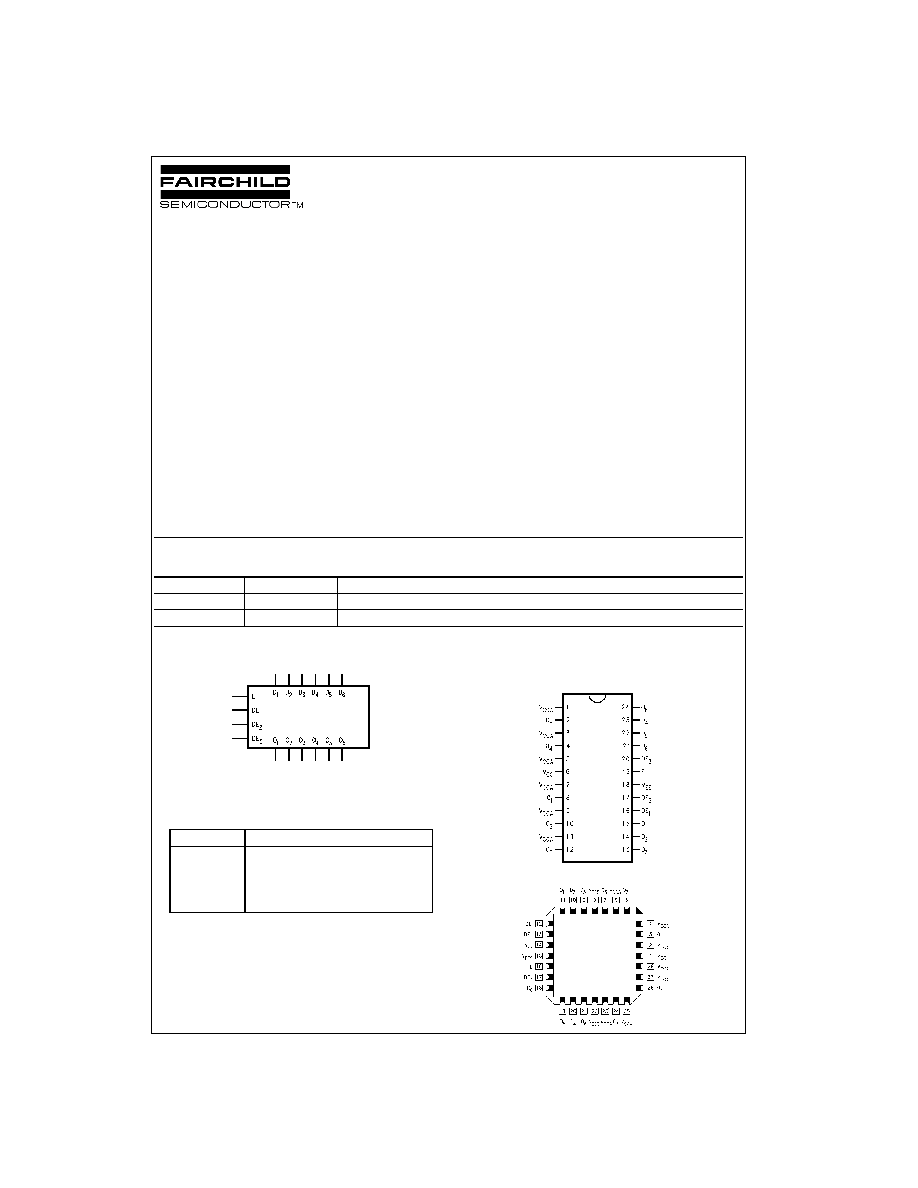
Logic Symbol
Pin Descriptions
Connection Diagrams
24-Pin DIP
28-Pin PLCC
Order Number
Package Number
Package Description
100323PC
N24E
24-Lead Plastic Dual-In-Line Package (PDIP), JEDEC MS-010, 0.400 Wide
100323QC
V28A
28-Lead Plastic Lead Chip Carrier (PLCC), JEDEC MO-047, 0.450 Square
Pin Names
Description
D
1
≠D
6
Data Inputs
DE
1
≠DE
3
Dual Enable Inputs
E
Common Enable Input
O
1
≠O
6
Data Outputs
www.fairchildsemi.com
2
100323
Truth Table
H
=
HIGH Voltage Level
L
=
LOW Voltage Level
X
=
Don't Care
Cutoff
=
Lower-than-LOW State
Logic Diagram
E
DE
n
D
n
D
n
+
1
O
n
O
n
+
1
L
L
X
X
Cutoff
Cutoff
X
H
L
L
Cutoff
Cutoff
X
H
L
H
Cutoff
H
X
H
H
L
H
Cutoff
X
H
H
H
H
H
H
X
L
L
Cutoff
Cutoff
H
X
L
H
Cutoff
H
H
X
H
L
H
Cutoff
H
X
H
H
H
H

3
www.fairchildsemi.com
1
00323
Absolute Maximum Ratings
(Note 1)
Recommended Operating
Conditions
Note 1: The "Absolute Maximum Ratings" are those values beyond which
the safety of the device cannot be guaranteed. The device should not be
operated at these limits. The parametric values defined in the Electrical
Characteristics tables are not guaranteed at the absolute maximum rating.
The "Recommended Operating Conditions" table will define the conditions
for actual device operation.
Note 2: ESD testing conforms to MIL-STD-883, Method 3015.
DC Electrical Characteristics
(Note 3)
V
EE
=
-
4.2V to
-
5.7V, V
CC
=
V
CCA
=
GND, T
C
=
0
∞
C to
+
85
∞
C
Note 3: The specified limits represent "worst case" values for the parameter. Since these values normally occur at the temperature extremes, additional
noise immunity and guardbanding can be achieved by decreasing the allowable system operating ranges. Conditions for testing shown in the tables are cho-
sen to guarantee operation under "worst case" conditions.
DIP AC Electrical Characteristics
(Note 4)
V
EE
=
-
4.2V to
-
5.7V, V
CC
=
V
CCA
=
GND
Note 4: The specified limits represent the "worst case" value for the parameter. Since these values normally occur at the temperature extremes, additional
noise immunity and guard banding can be achieved by decreasing the allowable system operating ranges. Conditions for testing shown in the tables are cho-
sen to guarantee operation under "worst case" conditions.
PLCC AC Electrical Characteristics
(Note 5)
V
EE
=
-
4.2V to
-
5.7V, V
CC
=
V
CCA
=
GND
Note 5: The specified limits represent the "worst case" value for the parameter. Since these values normally occur at the temperature extremes, additional
noise immunity and guard banding can be achieved by decreasing the allowable system operating ranges. Conditions for testing shown in the tables are cho-
sen to guarantee operation under "worst case" conditions.
Storage Temperature
-
65
∞
C to
+
150
∞
C
Maximum Junction Temperature
+
150
∞
C
V
EE
Pin Potential to Ground Pin
-
7.0V to
+
0.5V
Input Voltage (DC)
V
EE
to
+
0.5V
Output Current (DC Output High)
-
50 mA
ESD
2000V
Case Temperature
0
∞
C to
+
85
∞
C
Supply Voltage (V
EE
)
-
5.7V to
-
4.2V
Symbol
Parameter
Min
Typ
Max
Units
Conditions
V
IH
Input HIGH Voltage
-
1165
-
870
mV
Guaranteed High Signal for ALL Inputs
V
IL
Input LOW Voltage
-
1830
-
1475
mV
Guaranteed Low Signal for ALL Inputs
V
OH
Output HIGH Voltage
-
1025
-
955
-
870
mV
V
IN
=
V
IH (max)
or V
IL (min)
Loading with 25
to
-
2.0V
V
OHC
Output HIGH Voltage
-
1035
mV
V
IN
=
V
IH (min)
or V
IL (max)
Loading with 25
to
-
2.0V
V
OLZ
Cut-Off LOW Voltage
-
1950
mV
V
IN
=
V
IH (min)
or V
IL (max)
Loading with 25
to
-
2.0V
I
IL
Input LOW Current
0.50
µ
A
V
IN
=
V
IL (min)
I
IH
Input HIGH Current
240
µ
A
V
IN
=
V
IH (max)
I
EE
Power Supply Current
-
121
-
91
-
57
mA
Inputs Open
Symbol
Parameter
T
C
=
0
∞
C
T
C
=
+
25
∞
C
T
C
=
+
85
∞
C
Units
Conditions
Min
Max
Min
Max
Min
Max
t
PZH
Propagation Delay
1.90
3.60
1.90
3.60
2.00
3.80
ns
Figures 1, 2
t
PHZ
Data to Output
1.30
2.70
1.30
2.70
1.50
2.70
t
PZH
Propagation Delay
1.90
3.60
1.90
3.60
2.00
3.90
ns
t
PHZ
Dual Enable to Output
1.60
3.00
1.60
3.00
1.70
3.40
t
PZH
Propagation Delay
1.80
3.50
1.80
3.50
2.00
3.80
ns
t
PHZ
Common Enable to Output
1.50
2.90
1.50
2.90
1.60
3.00
t
TZH
Transition Time
0.50
1.80
0.50
1.80
0.50
1.80
ns
t
THZ
20% to 80%, 80% to 20%
0.35
1.40
0.35
1.40
0.35
1.40
Symbol
Parameter
T
C
=
0
∞
C
T
C
=
+
25
∞
C
T
C
=
+
85
∞
C
Units
Conditions
Min
Max
Min
Max
Min
Max
t
PZH
Propagation Delay
1.90
3.40
1.90
3.40
2.00
3.60
ns
Figures 1, 2
t
PHZ
Data to Output
1.30
2.50
1.30
2.50
1.50
2.70
t
PZH
Propagation Delay
1.90
3.40
1.90
3.40
2.00
3.70
ns
t
PHZ
Dual Enable to Output
1.60
2.80
1.60
2.80
1.70
3.00
t
PZH
Propagation Delay
1.80
3.30
1.80
3.30
2.00
3.60
ns
t
PHZ
Common Enable to Output
1.50
2.70
1.50
2.70
1.60
2.80
t
TZH
Transition Time
0.50
1.70
0.50
1.70
0.50
1.70
ns
t
THZ
20% to 80%, 80% to 20%
0.35
1.30
0.35
1.20
0.35
1.30

www.fairchildsemi.com
4
100323
Test Circuitry
Note:
∑
V
CC
, V
CCA
=
+
2V, V
EE
=
-
2.5V
∑
L1 and L2
=
equal length 50
impedance lines
∑
R
T
=
50
terminator internal to scope
∑
Decoupling 0.1
µ
F from GND to V
CC
and V
EE
∑
All unused outputs are loaded with 25
to GND
∑
C
L
=
Fixture and stray capacitance
3 pF
∑
Pin numbers shown are for flatpak; for DIP see logic symbol
FIGURE 1. AC Test Circuit
Timing Waveform
FIGURE 2. Propagation Delay and Transition Times

5
www.fairchildsemi.com
1
00323
Physical Dimensions
inches (millimeters) unless otherwise noted
24-Lead Plastic Dual-In-Line Package (PDIP), JEDEC MS-010, 0.400 Wide
Package Number N24E