 | –≠–ª–µ–∫—Ç—Ä–æ–Ω–Ω—ã–π –∫–æ–º–ø–æ–Ω–µ–Ω—Ç: 100341PC | –°–∫–∞—á–∞—Ç—å:  PDF PDF  ZIP ZIP |
© 2000 Fairchild Semiconductor Corporation
DS009880
www.fairchildsemi.com
July 1988
Revised August 2000
1
00341 Low
Power 8-Bi
t Shif
t Regi
ster
100341
Low Power 8-Bit Shift Register
General Description
The 100341 contains eight edge-triggered, D-type flip-flops
with individual inputs (P
n
) and outputs (Q
n
) for parallel
operation, and with serial inputs (D
n
) and steering logic for
bidirectional shifting. The flip-flops accept input data a
setup time before the positive-going transition of the clock
pulse and their outputs respond a propagation delay after
this rising clock edge.
The circuit operating mode is determined by the Select
inputs S
0
and S
1
, which are internally decoded to select
either "parallel entry", "hold", "shift left" or "shift right" as
described in the Truth Table. All inputs have 50 k
pull-
down resistors.
Features
s
35% power reduction of the 100141
s
2000V ESD protection
s
Pin/function compatible with 100141
s
Voltage compensated operating range
=
-
4.2V to
-
5.7V
s
Available to industrial grade temperature range
Ordering Code:
Devices also available in Tape and Reel. Specify by appending the suffix letter "X" to the ordering code.
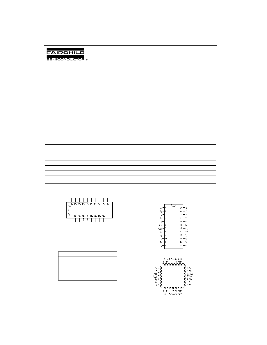
Logic Symbol
Pin Descriptions
Connection Diagrams
24-Pin DIP/SOIC
28-Pin PLCC
Order Number
Package Number
Package Description
10034SC
M24B
24-Lead Small Outline Integrated Circuit (SOIC), JEDEC MS-013, 0.300 Wide
100341PC
N24E
24-Lead Plastic Dual-In-Line Package (PDIP), JEDEC MS-010, 0.400 Wide
100341QI
V28A
28-Lead Plastic Lead Chip Carrier (PLCC), JEDEC MO-047, 0.450 Square
100341QC
V28A
28-Lead Plastic Lead Chip Carrier (PLCC), JEDEC MO-047, 0.450 Square
Industrial Temperature Range (
-
40
∞
C to
+
85
∞
C)
Pin Names
Description
CP
Clock Input
S
0
, S
1
Select Inputs
D
0
, D
7
Serial Inputs
P
0
≠P
7
Parallel Inputs
Q
0
≠Q
7
Data Outputs
www.fairchildsemi.com
2
100341
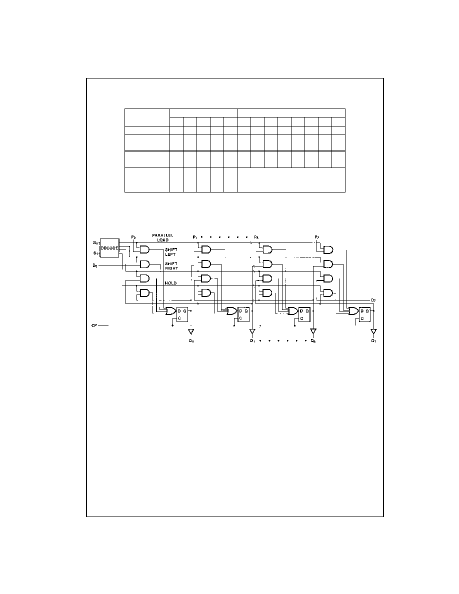
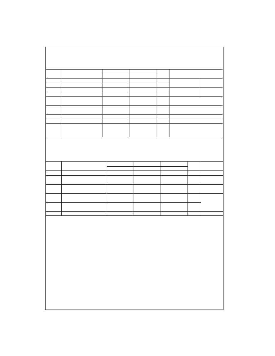
Truth Table
H
=
HIGH Voltage Level
L
=
LOW Voltage Level
X
=
Don't Care
=
LOW-to-HIGH Transition
Logic Diagram
Function
Inputs
Outputs
D
7
D
0
S
1
S
0
CP
Q
7
Q
6
Q
5
Q
4
Q
3
Q
2
Q
1
Q
0
Load Register
X
X
L
L
P
7
P
6
P
5
P
4
P
3
P
2
P
1
P
0
Shift Left
X
L
L
H
Q
6
Q
5
Q
4
Q
3
Q
2
Q
1
Q
0
L
Shift Left
X
H
L
H
Q
6
Q
5
Q
4
Q
3
Q
2
Q
1
Q
0
H
Shift Right
L
X
H
L
L
Q
7
Q
6
Q
5
Q
4
Q
3
Q
2
Q
1
Shift Right
H
X
H
L
H
Q
7
Q
6
Q
5
Q
4
Q
3
Q
2
Q
1
Hold
X
X
H
H
X
Hold
X
X
X
X
H
No Change
Hold
X
X
X
X
L
3
www.fairchildsemi.com
1
00341
Absolute Maximum Ratings
(Note 1)
Recommended Operating
Conditions
Note 1: The "Absolute Maximum Ratings" are those values beyond which
the safety of the device cannot be guaranteed. The device should not be
operated at these limits. The parametric values defined in the Electrical
Characteristics tables are not guaranteed at the absolute maximum rating.
The "Recommended Operating Conditions" table will define the conditions
for actual device operation.
Note 2: ESD testing conforms to MIL-STD-883, Method 3015.
Commercial Version
DC Electrical Characteristics
(Note 3)
V
EE
=
-
4.2V to
-
5.7V, V
CC
=
V
CCA
=
GND, T
C
=
0
∞
C to
+
85
∞
C
Note 3: The specified limits represent the "worst case" value for the parameter. Since these values normally occur at the temperature extremes, additional
noise immunity and guardbanding can be achieved by decreasing the allowable system operating ranges. Conditions for testing shown in the tables are cho-
sen to guarantee operation under "worst case" conditions.
DIP AC Electrical Characteristics
V
EE
=
-
4.2V to
-
5.7V, V
CC
=
V
CCA
=
GND
Note 4: The propagation delay specified is for the switching of a single output. Delays may vary up to 0.40 ns if multiple outputs are switching simultaneously.
Storage Temperature (T
STG
)
-
65
∞
C to
+
150
∞
C
Maximum Junction Temperature (T
J
)
+
150
∞
C
V
EE
Pin Potential to Ground Pin
-
7.0V to
+
0.5V
Input Voltage (DC)
V
EE
to
+
0.5V
Output Current (DC Output HIGH)
-
50 mA
ESD (Note 2)
2000V
Case Temperature (T
C
)
Commercial
0
∞
C to
+
85
∞
C
Industrial
-
40
∞
C to
+
85
∞
C
Supply Voltage (V
EE
)
-
5.7V to
-
4.2V
Symbol
Parameter
Min
Typ
Max
Units
Conditions
V
OH
Output HIGH Voltage
-
1025
-
955
-
870
mV
V
IN
=
V
IH
(Max)
Loading with
V
OL
Output LOW Voltage
-
1830
-
1705
-
1620
mV
or V
IL
(Min)
50
to
-
2.0V
V
OHC
Output HIGH Voltage
-
1035
mV
V
IN
=
V
IH
(Min)
Loading with
V
OLC
Output LOW Voltage
-
1610
mV
or V
IL
(Max)
50
to
-
2.0V
V
IH
Input HIGH Voltage
-
1165
-
870
mV
Guaranteed HIGH Signal
for all Inputs
V
IL
Input LOW Voltage
-
1830
-
1475
mV
Guaranteed LOW Signal
for all Inputs
I
IL
Input LOW Current
0.50
µ
A
V
IN
=
V
IL
(Min)
I
IH
Input HIGH Current
240
µ
A
V
IN
=
V
IH
(Max)
I
EE
Power Supply Current
Inputs OPEN
-
157
-
75
mA
V
EE
=
-
4.2V to
-
4.8V
-
167
-
75
mA
V
EE
=
-
4.2V to
-
5.7V
Symbol
Parameter
T
C
=
0
∞
C
T
C
=
+
25
∞
C
T
C
=
+
85
∞
C
Units
Conditions
Min
Max
Min
Max
Min
Max
f
MAX
Max Clock Frequency
400
400
400
MHz
Figures 2, 3
t
PLH
Propagation Delay
0.90
1.90
1.00
2.00
1.00
2.10
ns
Figures 1, 3
t
PHL
CP to Output
(Note 4)
t
TLH
Transition Time
0.35
1.30
0.35
1.30
0.35
1.30
ns
Figures 1, 3
t
THL
20% to 80%, 80% to 20%
t
S
Setup Time
D
n
, P
n
0.65
0.65
0.65
ns
Figure 4
S
n
1.60
1.60
1.60
t
H
Hold
D
n
, P
n
0.80
0.80
0.80
ns
S
n
0.60
0.60
0.60
t
PW
(H)
Pulse Width HIGH
CP
2.00
2.00
2.00
ns
Figure 3
www.fairchildsemi.com
4
100341
Commercial Version
(Continued)
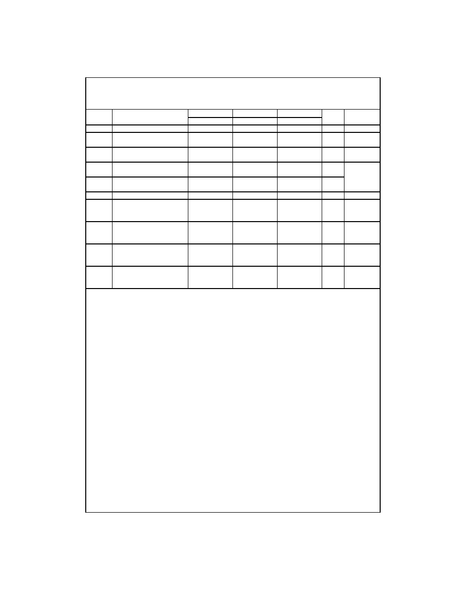
SOIC and PLCC AC Electrical Characteristics
V
EE
=
-
4.2V to
-
5.7V, V
CC
=
V
CCA
=
GND
Note 5: The propagation delay specified is for the switching of a single output. Delays may vary up to 0.40 ns if multiple outputs are switching simultaneously.
Note 6: Output-to-Output Skew is defined as the absolute value of the difference between the actual propagation delay for any outputs within the same pack-
aged device. The specifications apply to any outputs switching in the same direction either HIGH-to-LOW (t
OSHL
), or LOW-to-HIGH (t
OSLH
), or in opposite
directions both HL and LH (t
OST
). Parameters t
OST
and t
PS
guaranteed by design
Symbol
Parameter
T
C
=
0
∞
C
T
C
=
+
25
∞
C
T
C
=
+
85
∞
C
Units
Conditions
Min
Max
Min
Max
Min
Max
f
MAX
Maximum Clock Frequency
425
425
425
MHz
Figures 2, 3
t
PLH
Propagation Delay
0.90
1.70
1.00
1.80
1.00
1.90
ns
Figures 1, 3
t
PHL
CP to Output
(Note 5)
t
TLH
Transition Time
0.35
1.20
0.35
1.20
0.35
1.20
ns
Figures 1, 3
t
THL
20% to 80%, 80% to 20%
t
S
Setup Time
D
n
, P
n
0.55
0.55
0.55
ns
S
n
1.50
1.50
1.50
Figure 4
t
H
Hold Time
D
n
, P
n
0.70
0.70
0.70
ns
S
n
0.50
0.50
0.50
t
PW
(H)
Pulse Width HIGH
CP
2.00
2.00
2.00
ns
Figure 3
t
OSHL
Maximum Skew Common Edge
PLCC Only
Output-to-Output Variation
200
200
200
ps
(Note 6)
Clock to Output Path
t
OSLH
Maximum Skew Common Edge
PLCC Only
Output-to-Output Variation
200
200
200
ps
(Note 6)
Clock to Output Path
t
OST
Maximum Skew Opposite Edge
PLCC Only
Output-to-Output Variation
250
250
250
ps
(Note 6)
Clock to Output Path
t
ps
Maximum Skew
PLCC Only
Pin (Signal) Transition Variation
250
250
250
ps
(Note 6)
Clock to Output Path
5
www.fairchildsemi.com
1
00341
Industrial Version
PLCC DC Electrical Characteristics
(Note 7)
V
EE
=
-
4.2V to
-
5.7V, V
CC
=
V
CCA
=
GND, T
C
=
-
40
∞
C to
+
85
∞
C
Note 7: The specified limits represent the "worst case" value for the parameter. Since these values normally occur at the temperature extremes, additional
noise immunity and guardbanding can be achieved by decreasing the allowable system operating ranges. Conditions for testing shown in the tables are cho-
sen to guarantee operation under "worst case" conditions.
PLCC AC Electrical Characteristics
V
EE
=
-
4.2V to
-
5.7V, V
CC
=
V
CCA
=
GND
Note 8: The propagation delay specified is for the switching of a single output. Delays may vary up to 0.40 ns if multiple outputs are switching simultaneously.
Symbol
Parameter
T
C
=
-
40
∞
C
T
C
=
0
∞
C to
+
85
∞
C
Units
Conditions
Min
Max
Min
Max
V
OH
Output HIGH Voltage
-
1085
-
870
-
1025
-
870
mV
V
IN
=
V
IH
(Max)
Loading with
V
OL
Output LOW Voltage
-
1830
-
1575
-
1830
-
1620
mV
or V
IL
(Min)
50
to
-
2.0V
V
OHC
Output HIGH Voltage
-
1095
-
1035
mV
V
IN
=
V
IH
(Min)
Loading with
V
OLC
Output LOW Voltage
-
1565
-
1610
mV
or V
IL
(Max)
50
to
-
2.0V
V
IH
Input HIGH Voltage
-
1170
-
870
-
1165
-
870
mV
Guaranteed HIGH Signal
for all Inputs
V
IL
Input LOW Voltage
-
1830
-
1480
-
1830
-
1475
mV
Guaranteed LOW Signal
for all Inputs
I
IL
Input LOW Current
0.50
0.50
µ
A
V
IN
=
V
IL
(Min)
I
IH
Input HIGH Current
240
240
µ
A
V
IN
=
V
IH
(Max)
I
EE
Power Supply Current
Inputs OPEN
-
157
-
75
-
157
-
75
mA
V
EE
=
-
4.2V to
-
4.8V
-
167
-
75
-
167
-
75
mA
V
EE
=
-
4.2V to
-
5.7V
Symbol
Parameter
T
C
=
-
40
∞
C
T
C
=
+
25
∞
C
T
C
=
+
85
∞
C
Units
Conditions
Min
Max
Min
Max
Min
Max
f
MAX
Max Clock Frequency
425
425
425
MHz
Figures 2, 3
t
PLH
Propagation Delay
0.90
1.80
1.00
1.80
1.00
1.90
ns
Figures 1, 3
t
PHL
CP to Output
(Note 8)
t
TLH
Transition Time
0.30
1.90
0.35
1.20
0.35
1.20
ns
Figures 1, 3
t
THL
20% to 80%, 80% to 20%
t
S
Setup Time
D
n
, P
n
0.60
0.55
0.55
ns
S
n
1.70
1.50
1.50
Figure 4
t
H
Hold Time
D
n
, P
n
0.90
0.70
0.70
ns
S
n
0.50
0.50
0.50
t
PW
(H)
Pulse Width HIGH
CP
2.00
2.00
2.00
ns
Figure 3