 | –≠–ª–µ–∫—Ç—Ä–æ–Ω–Ω—ã–π –∫–æ–º–ø–æ–Ω–µ–Ω—Ç: 100395 | –°–∫–∞—á–∞—Ç—å:  PDF PDF  ZIP ZIP |

© 1999 Fairchild Semiconductor Corporation
DS010651
www.fairchildsemi.com
February 1990
Revised November 1999
1
00395 Low
Power 9-Bi
t ECL-t
o
-TTL
T
r
anslat
or wit
h
Regi
st
ers
100395
Low Power 9-Bit ECL-to-TTL Translator with Registers
General Description
The 100395 is a 9-bit translator for converting F100K logic
levels to TTL logic levels. A HIGH on the output enable
(OE) holds the TTL outputs in a high impedance state. Two
separate clock inputs are available for multiplexing and
system level testing.
The 100395 is designed with TTL 64 mA outputs for bus
driving capability. All inputs have 50 k
pull down resistors.
When the inputs are either unconnected or at the same
potential, the outputs will go LOW.
Features
s
64 mA I
OL
drive capability
s
2000V ESD protection
s
-
4.2V to
-
5.7V operating range
s
Registered outputs
s
TTL outputs
Ordering Code:
Devices also available in Tape and Reel. Specify by appending the suffix letter "X" to the ordering code.
Logic Symbol
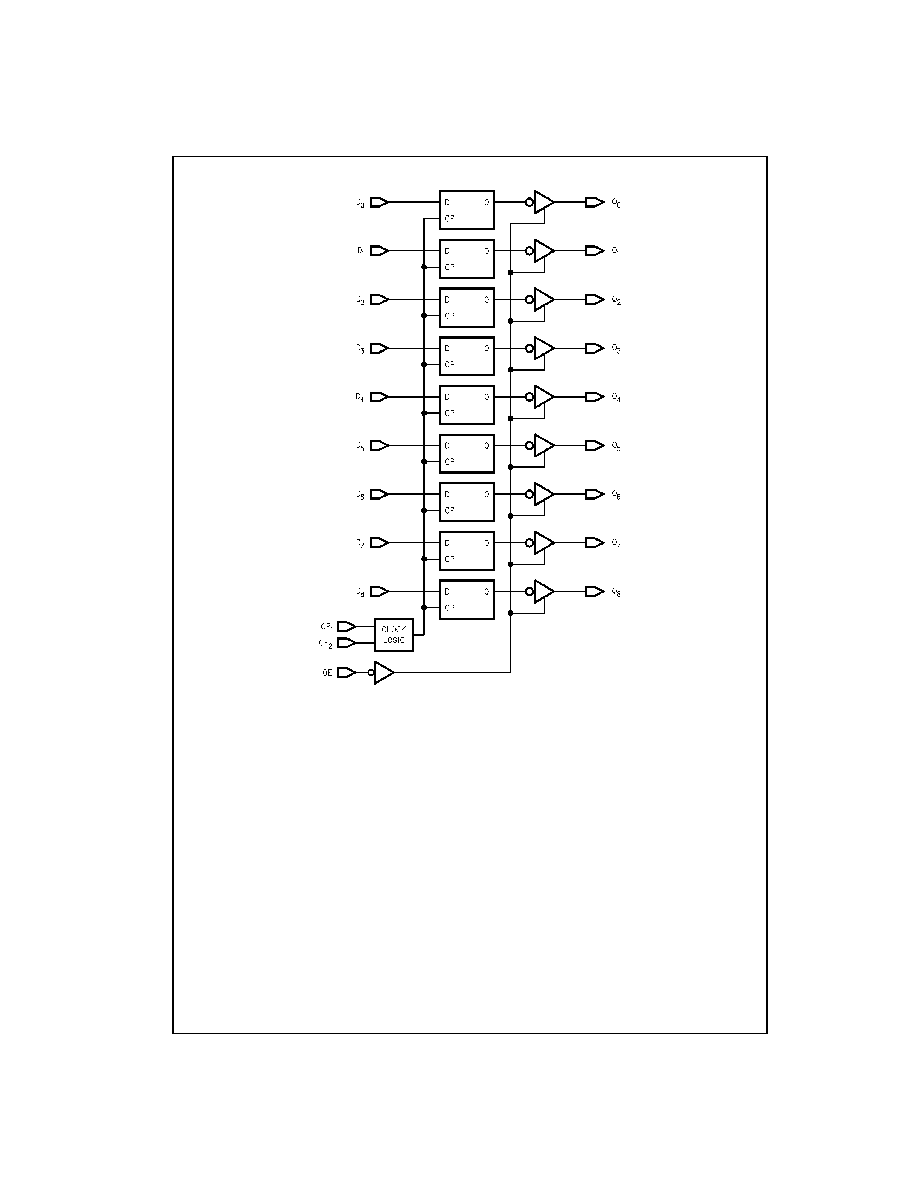
Pin Descriptions
Connection Diagram
Truth Table
H
=
HIGH Voltage Level
Z
=
High Impedance
L
=
LOW Voltage Level
NC
=
No Change
X
=
Don't Care
Order Number
Package Number
Package Description
100395QC
V28A
28-Lead Plastic Lead Chip Carrier (PLCC), JEDEC MO-047, 0.450 Square
Pin Names
Description
D
0
≠D
8
Data Inputs (ECL)
Q
0
≠Q
8
Data Outputs (TTL)
OE
Output Enable (ECL)
CP
1
, CP
2
Clock Inputs (ECL)
Inputs
Outputs
CP
1
CP
2
OE
D
N
Q
N
L
L
L
L
L
L
L
L
L
L
H
H
L
L
H
H
H
X
X
X
NC
X
H
X
X
NC
L
L
X
X
NC
X
X
H
X
Z
www.fairchildsemi.com
2
100395
Logic Diagram

3
www.fairchildsemi.com
1
00395
Absolute Maximum Ratings
(Note 1)
Recommended Operating
Conditions
Note 1: The "Absolute Maximum Ratings" are those values beyond which
the safety of the device cannot be guaranteed. The device should not be
operated at these limits. The parametric values defined in the Electrical
Characteristics tables are not guaranteed at the absolute maximum rating.
The "Recommended Operating Conditions" table will define the conditions
for actual device operation.
Note 2: ESD testing conforms to MIL-STD-883, Method 3015.
Commercial Version
DC Electrical Characteristics
(Note 3)
V
EE
=
-
4.2V to
-
5.7V, V
CC
=
V
CCA
=
GND, T
C
=
0
∞
C to
+
85
∞
C
Note 3: The specified limits represent the "worst case" value for the parameter. Since these values normally occur at the temperature extremes, additional
noise immunity and guardbanding can be achieved by decreasing the allowable system operating ranges. Conditions for testing shown in the tables are cho-
sen to guarantee operation under "worst case" conditions.
PLCC AC Electrical Characteristics
V
EE
=
-
4.2V to
-
5.7V, V
CC
=
GND, V
TTL
=
+
4.5V to
+
5.5V
Storage Temperature (T
STG
)
-
65
∞
C to
+
150
∞
C
Maximum Junction Temperature (T
J
)
+
150
∞
C
Case Temperature under Bias (T
C
)
0
∞
C to
+
85
∞
C
V
EE
Pin Potential to Ground Pin
-
7.0V to
+
0.5V
V
TTL
Pin Potential to Ground Pin
-
0.5V to
+
6.0V
ECL Input Voltage (DC)
V
EE
to
+
0.5V
TTL Input Voltage
-
0.5V to
+
7.0V
Output Current
(DC Output HIGH)
+
130 mA
ESD (Note 2)
2000V
Case Temperature (T
C
)
0
∞
C to
+
85
∞
C
Supply Voltage
V
EE
-
5.7V to
-
4.2V
V
TTL
+
4.5V to
+
5.5V
Symbol
Parameter
Min
Typ
Max
Units
Conditions
V
OH
Output HIGH Voltage
2.4
V
I
OH
=
-
15 mA
V
IN
=
V
IH
(Max)
V
OL
Output LOW Voltage
0.55
V
I
OL
=
64 mA
or V
IL
(Min)
V
IH
Input HIGH Voltage
-
1165
-
870
mV
Guaranteed HIGH Signal for All Inputs
V
IL
Input LOW Voltage
-
1830
-
1475
mV
Guaranteed LOW Signal for All Inputs
I
IL
Input LOW Current
0.5
µ
A
V
IN
=
V
IL
(Min)
I
IH
Input HIGH Current
240
µ
A
V
IN
=
V
IH
(Max)
I
OZL
3-STATE Current Output HIGH
-
50
µ
A
V
OUT
=
+
0.4V
I
OZH
3-STATE Current Output LOW
+
50
µ
A
V
OUT
=
+
2.7V
I
CEX
Output HIGH Leakage Current
250
µ
A
V
OUT
=
V
CC
I
OS
Output Short-Circuit Current
-
100
-
225
mA
I
EE
V
EE
Power Supply Current
-
67
-
29
mA
Inputs OPEN
I
CCH
V
TTL
Power Supply Current HIGH
29
mA
I
CCL
V
TTL
Power Supply Current LOW
65
mA
I
CCZ
V
TTL
Power Supply Current 3-STATE
49
mA
Symbol
Parameter
T
C
=
0
∞
C
T
C
=
+
25
∞
C
T
C
=
+
85
∞
C
Units
Conditions
Min
Max
Min
Max
Min
Max
t
PLH
Propagation Delay
2.30
5.00
2.30
5.00
2.30
5.00
ns
Figures 1, 2
t
PHL
Clock to Output
3.00
5.60
3.00
5.60
3.40
6.40
t
PZL
Output Enable Time
3.20
7.60
3.20
7.60
3.20
7.60
ns
Figures 1, 3
t
PZH
OE
to Q
N
2.40
5.60
2.40
5.60
2.40
5.60
t
PLZ
Output Disable Time
3.20
7.60
3.20
7.60
3.20
7.60
ns
Figures 1, 3
t
PHZ
OE
to Q
N
2.40
5.60
2.40
5.60
2.40
5.60
t
H
Data to CP EN
1.5
1.5
1.5
ns
Figures 1, 2
Hold Time
1.5
1.5
1.5
t
S
Data to CP EN
0.5
0.5
0.5
ns
Figures 1, 2
Setup Time
0.5
0.5
0.5
t
PW
(H)
Clock Pulse Width
2.0
2.0
2.0
ns
Figures 1Figure 2
www.fairchildsemi.com
4
100395
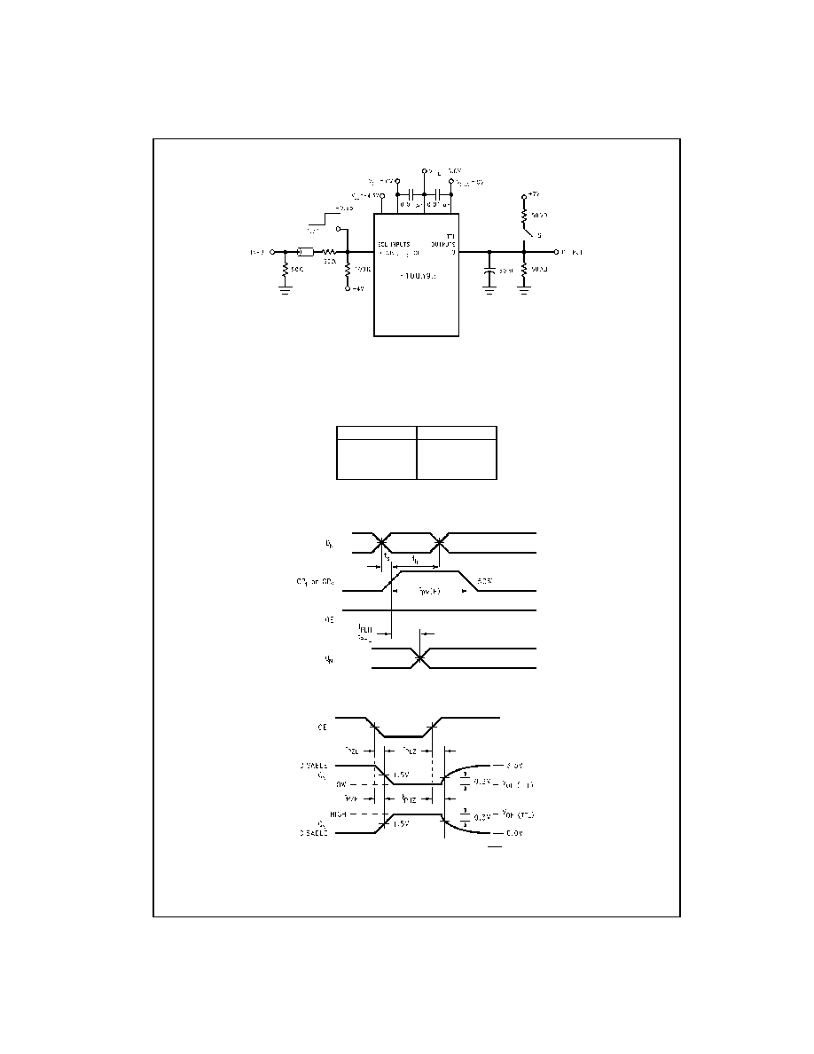
Test Circuit
Notes:
V
CC
=
0V, V
CCA
=
0V, V
EE
=
-
4.5V, V
TTL
=
+
5V.
All unused outputs are loaded with 500
to GND. Decoupling capacitors are necessary in the test and end application environment. When V
CC
and V
CCA
are
common to a single power plane, typically 0.0V, decouple V
TTL
to that plane with one 0.01
µ
F capacitor.
FIGURE 1. AC Test Circuit
Switch Positions for Parameter Testing
Switching Waveforms
FIGURE 2. Propagation Delay and Transition Times
FIGURE 3. Enable and Disable Waveforms, OE to Q
N
Parameter
S-Position
t
PLH
, t
PHL
Open
t
PHZ
, t
PZH
Open
t
PLZ
, t
PZL
Closed

5
www.fairchildsemi.com
1
00395 Low
Power 9-Bi
t ECL-t
o
-TTL
T
r
anslat
or wit
h
Regi
st
ers
Physical Dimensions
inches (millimeters) unless otherwise noted
28-Lead Plastic Lead Chip Carrier (PLCC), JEDEC MO-047, 0.450 Square
Package Number V28A
Fairchild does not assume any responsibility for use of any circuitry described, no circuit patent licenses are implied and
Fairchild reserves the right at any time without notice to change said circuitry and specifications.
LIFE SUPPORT POLICY
FAIRCHILD'S PRODUCTS ARE NOT AUTHORIZED FOR USE AS CRITICAL COMPONENTS IN LIFE SUPPORT
DEVICES OR SYSTEMS WITHOUT THE EXPRESS WRITTEN APPROVAL OF THE PRESIDENT OF FAIRCHILD
SEMICONDUCTOR CORPORATION. As used herein:
1. Life support devices or systems are devices or systems
which, (a) are intended for surgical implant into the
body, or (b) support or sustain life, and (c) whose failure
to perform when properly used in accordance with
instructions for use provided in the labeling, can be rea-
sonably expected to result in a significant injury to the
user.
2. A critical component in any component of a life support
device or system whose failure to perform can be rea-
sonably expected to cause the failure of the life support
device or system, or to affect its safety or effectiveness.
www.fairchildsemi.com