© 2003 Fairchild Semiconductor Corporation
DS500776
www.fairchildsemi.com
January 2003
Revised February 2003
1
00L
V
E
L1
6 3.
3V ECL
Dif
f
er
enti
al
Recei
ver
100LVEL16
3.3V ECL Differential Receiver
General Description
The 100LVEL16 is a low voltage differential receiver that
contains an internally supplied voltage source, V
BB
. When
used in a single ended input condition the unused input
must be tied to V
BB
. When operating in this mode use a
0.01
µ
F capacitor to decouple V
BB
and V
CC
and also limit
the current sinking or sourcing capability to 0.5mA. When
V
BB
is not used it should be left open.
With inputs open the differential Q outputs default LOW
and Q outputs default HIGH.
The 100 series is temperature compensated.
Features
s
Typical propagation delay of 300 ps
s
Typical I
EE
of 17 mA
s
Internal pull-down resistors on D
s
Fairchild MSOP-8 package is a drop-in replacement to
ON TSSOP-8
s
Meets or exceeds JEDEC specification EIA/JESD78 IC
latch-up test
s
Moisture Sensitivity Level 1
s
ESD Performance:
Human Body Model
>
2000V
Machine Model
>
150V
Ordering Code:
Devices also available in Tape and Reel. Specify by appending suffix letter "X" to the ordering code.
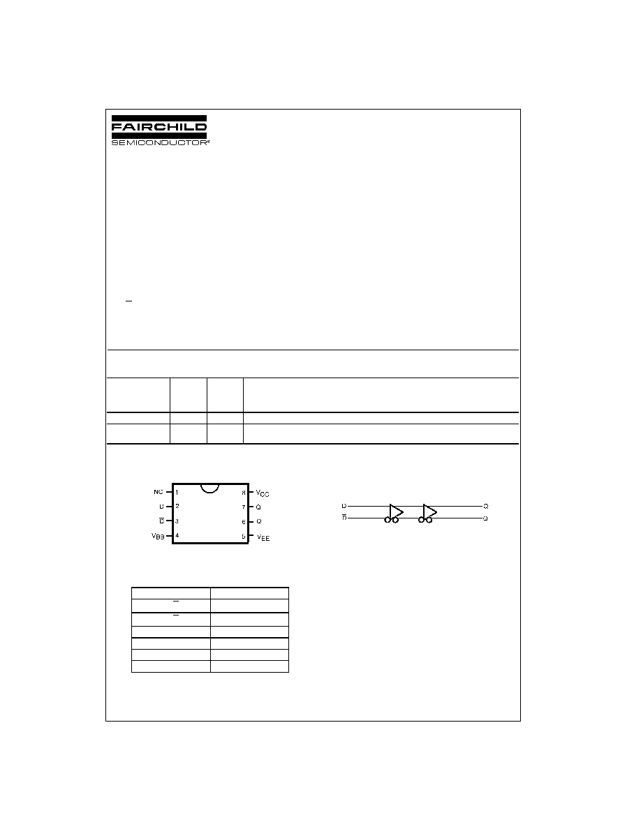
Connection Diagram
Top View
Pin Descriptions
Logic Diagram
Order Number
Product
Package Description
Package
Code
Number
Top Mark
100LVEL16M
M08A
KVL16
8-Lead Small Outline Integrated Circuit (SOIC), JEDEC MS-012, 0.150" Narrow
100LVEL16M8
(Preliminary)
MA08D
KV16
8-Lead Molded Small Outline Package (MSOP), JEDEC MO-187, 3.0mm Wide
Pin Name
Description
Q, Q
ECL Data Outputs
D, D
ECL Data Inputs
V
BB
Reference Voltage
V
CC
Positive Supply
V
EE
Negative Supply
NC
No Connect
www.fairchildsemi.com
2
10
0L
VEL16
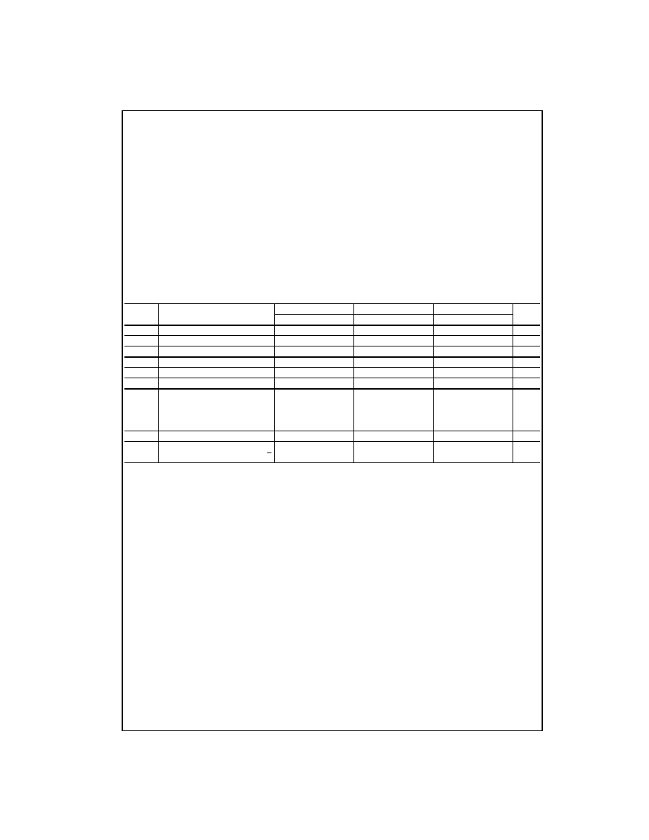
Absolute Maximum Ratings
(Note 1)
Recommended Operating
Conditions
Note 1: The "Absolute Maximum Ratings" are those values beyond which
the safety of the device cannot be guaranteed. The device should not be
operated at these limits. The parametric values defined in the Electrical
Characteristics tables are not guaranteed at the absolute maximum rating.
The "Recommended Operating Conditions" table will define the conditions
for actual device operation.
LVPECL DC Electrical Characteristics
V
CC
=
3.3V; V
EE
=
0.0V (Note 2)
Note 2: Input and output parameters vary 1 to 1 with V
CC
. V
EE
can vary
±
0.3V.
Note 3: Outputs are terminated through a 50
Resistor to V
CC
-
2.0V.
Note 4: V
IHCMR
minimum varies 1 to 1 with V
EE
. V
IHCMR
maximum varies 1 to 1 with V
CC
. The V
IHCMR
range is referenced to the most positive side of the dif-
ferential input signal. Normal operation is obtained if the HIGH level falls within the specified range and the peak-to-peak voltage lies between V
PPMIN
and
1V.
Note 5: Absolute value of the input HIGH and LOW current should not exceed the absolute value of the stated Min or Max specification.
Note: Devices are designed to meet the DC specifications after thermal equilibrium has been established. Circuit is tested with air flow greater than
500LFPM maintained.
PECL Supply Voltage (V
CC
) V
EE
=
0V
0.0V to
+
8.0V
NECL Supply Voltage (V
EE
) V
CC
=
0V
0.0V to
-
8.0V
PECL DC Input Voltage (V
I
) V
EE
=
0V
0.0V to
+
6.0V
NECL DC Input Voltage (V
I
) V
CC
=
0V
0.0V to
-
6.0V
DC Output Current (I
OUT
)
Continuous
50 mA
Surge
100 mA
V
BB
Sink/Source Current (I
BB
)
±
0.5 mA
Storage Temperature (T
STG
)
-
65
∞
C to
+
150
∞
C
PECL Power Supply
(V
EE
=
0V)
V
CC
=
3.0V to 3.8V
NECL Power Supply
(V
CC
=
0V)
V
EE
=
-
3.8V to
-
3.0V
Free Air Operating Temperature (T
A
)
-
40
∞
C to
+
85
∞
C
Symbol
Parameter
-
40
∞
C
25
∞
C
85
∞
C
Units
Min
Typ
Max
Min
Typ
Max
Min
Typ
Max
I
EE
Power Supply Current
17
23
17
23
18
24
mA
V
OH
Output HIGH Voltage (Note 3)
2215
2295
2420
2275
2345
2420
2275
2345
2420
mV
V
OL
Output LOW Voltage (Note 3)
1470
1605
1745
1490
1595
1680
1490
1595
1680
mV
V
IH
Input HIGH Voltage (Single Ended)
2135
2420
2135
2420
2135
2420
mV
V
IL
Input LOW Voltage (Single Ended)
1490
1825
1490
1825
1490
1825
mV
V
BB
Output Voltage Reference
1.92
2.04
1.92
2.04
1.92
2.04
V
V
IHCMR
Input HIGH Voltage Common Mode
Range (Differential) (Note 4)
V
PP
<
500mV
1.2
2.9
1.1
2.9
1.1
2.9
V
V
PP
500mV
1.5
2.9
1.4
2.9
1.4
2.9
I
IH
Input HIGH Current (Note 5)
150
150
150
µ
A
I
IL
Input LOW Current (Note 5)
D
0.5
0.5
0.5
µ
A
D
-
600
-
600
-
600
3
www.fairchildsemi.com
1
00L
V
E
L1
6
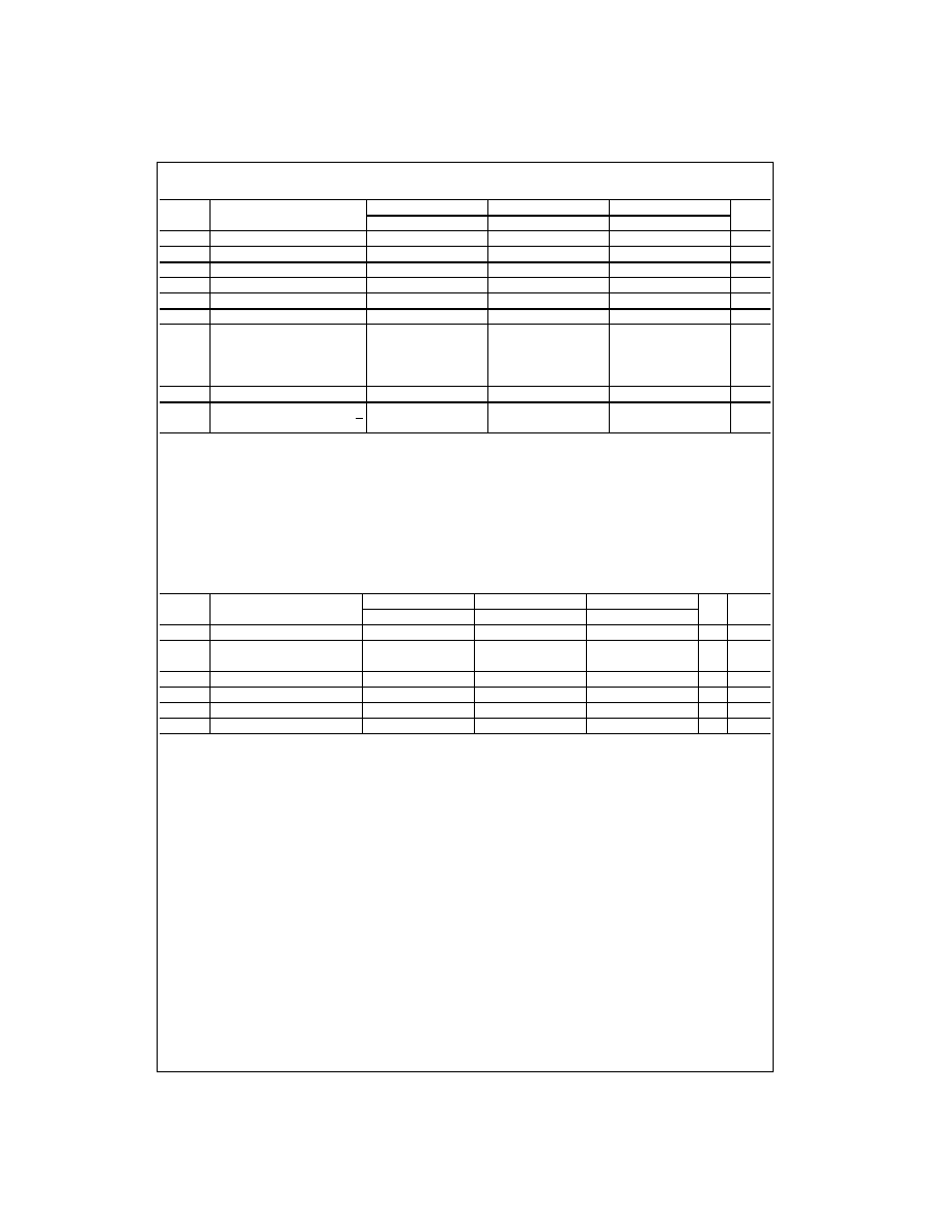
LVNECL DC Electrical Characteristics
V
CC
=
0.0V; V
EE
=
-
3.3V (Note 6)
Note 6: Input and output parameters vary 1 to 1 with V
CC
. V
EE
can vary
±
0.3V.
Note 7: Outputs are terminated through a 50
Resistor to V
CC
-
2.0V.
Note 8: V
IHCMR
minimum varies 1 to 1 with V
EE
. V
IHCMR
maximum varies 1-to-1 with V
CC
. The V
IHCMR
range is referenced to the most positive side of the
differential input signal. Normal operation is obtained if the HIGH level falls within the specified range and the peak-to-peak voltage lies between V
PPMIN
and
1V.
Note 9: Absolute value of the input HIGH and LOW current should not exceed the absolute value of the stated Min or Max specification.
Note: Devices are designed to meet the DC specifications after thermal equilibrium has been established. Circuit is tested with air flow greater than
500LFPM maintained.
100LVEL16 AC Electrical Characteristics
V
CC
=
3.3V; V
EE
=
0.0V or V
CC
=
0.0V; V
EE
=
-
3.3V
(Note 10) (Note 11)
Note 10: V
EE
can vary
±
0.3V.
Note 11: Measured using a 750 mV input swing centered at V
CC
- 1.32V; 50% duty cycle clock source; t
r
=
t
f
=
250 ps (20% - 80%) at f
IN
=
1 MHz. All loading
with 50
to V
CC
-
2.0V.
Note 12: Duty cycle skew is the difference between a t
PLH
and t
PHL
propagation delay through a device under identical conditions.
Symbol
Parameter
-
40
∞
C
25
∞
C
85
∞
C
Units
Min
Typ
Max
Min
Typ
Max
Min
Typ
Max
I
EE
Power Supply Current
17
23
17
23
18
24
mA
V
OH
Output HIGH Voltage (Note 7)
-
1085
-
1005
-
880
-
1025
-
955
-
880
-
1025
-
955
-
880
mV
V
OL
Output LOW Voltage (Note 7)
-
1830
-
1695
-
1555
-
1810
-
1705
-
1620
-
1810
-
1705
-
1620
mV
V
IH
Input HIGH Voltage (Single Ended)
-
1165
-
880
-
1165
-
880
-
1165
-
880
mV
V
IL
Input LOW Voltage (Single Ended)
-
1810
-
1475
-
1810
-
1475
-
1810
-1475
mV
V
BB
Output Voltage Reference
-
1.38
-
1.26
-
1.38
-
1.26
-
1.38
-
1.26
V
V
IHCMR
Input HIGH Voltage Common Mode
Range (Differential) (Note 8)
V
PP
<
500mV
-
2.5
-
0.4
-
2.5
-
0.4
-
2.5
-
0.4
V
V
PP
500mV
-
1.8
-
0.4
-
1.9
-
0.4
-
1.9
-
0.4
I
IH
Input HIGH Current
150
150
150
µ
A
I
IL
Input LOW Current
D
0.5
0.5
0.5
µ
A
D
-
600
-
600
-
600
Symbol
Parameter
-
40
∞
C
25
∞
C
85
∞
C
Units
Figure
Min
Typ
Max
Min
Typ
Max
Min
Typ
Max
Number
f
MAX
Maximum Toggle Frequency
TBD
TBD
TBD
GHz
t
PLH
, t
PHL
Propagation Delay to Output (Diff)
150
275
400
225
300
375
240
315
390
ps
Figures
1, 3
(SE)
100
275
450
175
300
425
190
315
440
t
SKEW
Duty Cycle Skew (Note 12)
5
30
5
20
5
20
ps
t
JITTER
Cycle-to-Cycle Jitter
TBD
TBD
TBD
ps
V
PP
Input Swing
150
1000
150
1000
150
1000
mV
Figure 1
t
r
, t
f
Output Rise Times Q (20% to 80%)
120
220
320
120
220
320
120
220
320
ps
Figure 2
www.fairchildsemi.com
4
10
0L
VEL16
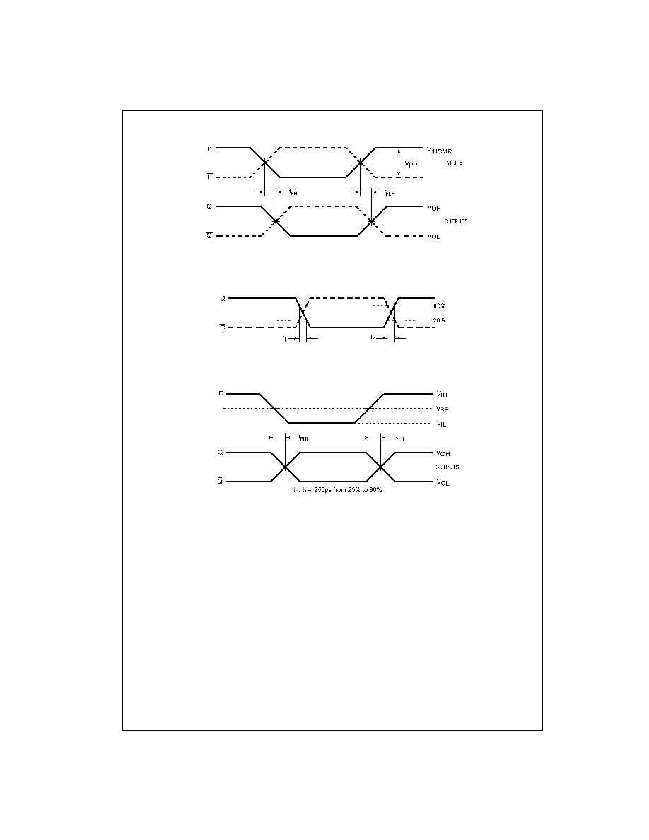
Switching Waveforms
FIGURE 1. Differential to Differential Propagation Delay
FIGURE 2. Differential Output Edge Rates
FIGURE 3. Single Ended to Differential Propagation Delay

5
www.fairchildsemi.com
1
00L
V
E
L1
6
Physical Dimensions
inches (millimeters) unless otherwise noted
8-Lead Small Outline Integrated Circuit (SOIC), JEDEC MS-012, 0.150" Narrow
Package Number M08A