2N3663
Discrete POWER & Signal
Technologies
NPN RF Transistor
2N3663
Absolute Maximum Ratings*
TA = 25∞C unless otherwise noted
*
These ratings are limiting values above which the serviceability of any semiconductor device may be impaired.
NOTES:
1) These ratings are based on a maximum junction temperature of 150 degrees C.
2) These are steady state limits. The factory should be consulted on applications involving pulsed or low duty cycle operations.
Thermal Characteristics
TA = 25∞C unless otherwise noted
Symbol
Parameter
Value
Units
V
CEO
Collector-Emitter Voltage
12
V
V
CBO
Collector-Base Voltage
30
V
V
EBO
Emitter-Base Voltage
3.0
V
I
C
Collector Current - Continuous
50
mA
T
J
, T
stg
Operating and Storage Junction Temperature Range
-55 to +150
∞
C
Symbol
Characteristic
Max
Units
2N3663
P
D
Total Device Dissipation
Derate above 25
∞
C
350
2.8
mW
mW/
∞
C
R
JC
Thermal Resistance, Junction to Case
125
∞
C/W
R
JA
Thermal Resistance, Junction to Ambient
357
∞
C/W
E
C
B
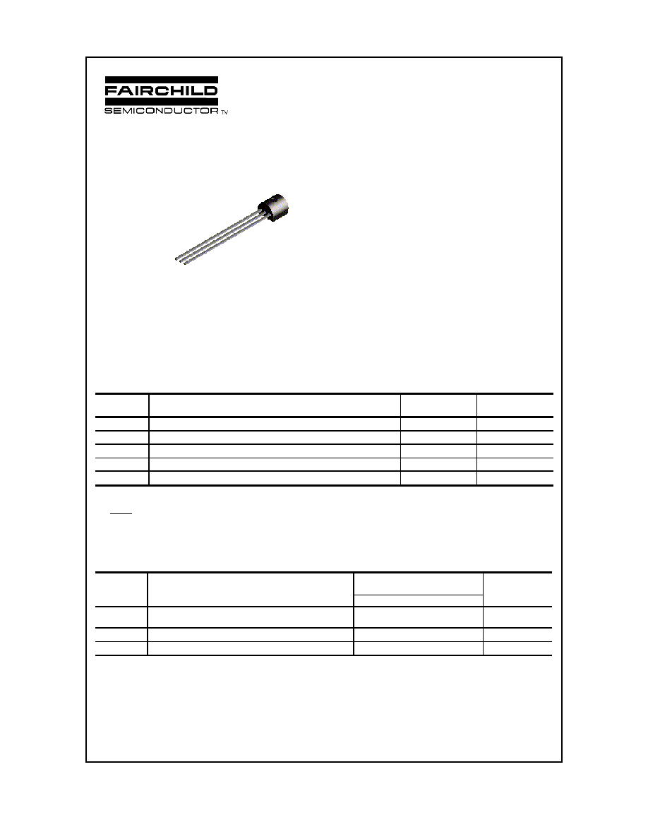
TO-92
This device is designed for use as RF amplifiers, oscillators and
multipliers with collector currents in the 1.0 mA to 30 mA range.
Sourced from Process 43. See PN918 for characteristics.
©
1997 Fairchild Semiconductor Corporation
2N3663
NPN RF Transistor
(continued)
Electrical Characteristics
TA = 25∞C unless otherwise noted
OFF CHARACTERISTICS
Symbol
Parameter
Test Conditions
Min
Max
Units
V
(BR)CEO
Collector-Emitter Breakdown Voltage*
I
C
= 1.0 mA, I
B
= 0
12
V
V
(BR)CBO
Collector-Base Breakdown Voltage
I
C
= 100
µ
A, I
E
= 0
30
V
V
(BR)EBO
Emitter-Base Breakdown Voltage
I
E
= 100
µ
A, I
C
= 0
3.0
V
I
CBO
Collector-Cutoff Current
V
CB
= 15 V, I
E
= 0
0.5
µ
A
I
EBO
Emitter-Cutoff Current
V
EB
= 2.0 V, I
C
= 0
0.5
µ
A
ON CHARACTERISTICS*
h
FE
DC Current Gain
V
CE
= 10 V, I
C
= 8.0 mA
20
*
Pulse Test: Pulse Width
300
µ
s, Duty Cycle
2.0%
SMALL SIGNAL CHARACTERISTICS
f
T
Current Gain - Bandwidth Product
I
C
= 5.0 mA, V
CE
= 10 V,
f = 100 MHz
700
2100
MHz
C
ob
Output Capacitance
V
CB
= 10 V, I
E
= 0, f = 1.0 MHz
0.8
1.7
pF
rb'C
C
Collector Base Time Constant
I
C
= 8.0 mA, V
CE
= 10 V,
f = 79.8 MHz
80
pS
FUNCTIONAL TEST
NF
Noise Figure
I
C
= 1.0 mA, V
CE
= 6.0 V,
f = 60 MHz, Rg = 400
6.5
dB
G
pe
Amplifier Power Gain
I
C
= 6.0 mA, V
CE
= 12 V,
f = 200 MHz
1.5
dB