 | –≠–ª–µ–∫—Ç—Ä–æ–Ω–Ω—ã–π –∫–æ–º–ø–æ–Ω–µ–Ω—Ç: 4528B | –°–∫–∞—á–∞—Ç—å:  PDF PDF  ZIP ZIP |

© 2000 Fairchild Semiconductor Corporation
DS005998
www.fairchildsemi.com
October 1987
Revised August 2000
CD452
8BC
Dual
Monost
a
ble Mult
ivi
b
ra
tor
CD4528BC
Dual Monostable Multivibrator
General Description
The CD4528B is a dual monostable multivibrator. Each
device is retriggerable and resettable. Triggering can occur
from either the rising or falling edge of an input pulse,
resulting in an output pulse over a wide range of widths.
Pulse duration and accuracy are determined by external
timing components Rx and Cx.
Features
s
Wide supply voltage range:
3.0V to 18V
s
Separate reset available
s
Quiescent current
=
5.0 nA/package (typ.) at 5.0 V
DC
s
Diode protection on all inputs
s
Triggerable from leading or trailing edge pulse
s
Capable of driving two low-power TTL loads or one low-
power Schottky TTL load over the rated temperature
range
Ordering Code:
Devices also available in Tape and Reel. Specify by appending the suffix letter "X" to the ordering code.
Connection Diagram
Top View
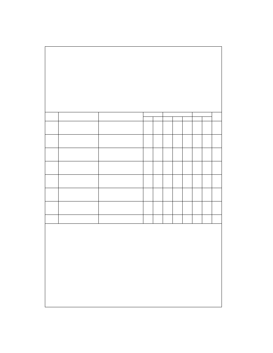
Truth Table
H
=
HIGH Level
L
=
LOW Level
=
Transition from LOW-to-HIGH
=
Transition from HIGH-to-LOW
�
=
One HIGH Level Pulse
=
One LOW Level Pulse
X
=
Irrelevant
Order Number
Package Number
Package Description
CD4528BCM
M16A
16-Lead Small Outline Integrated Circuit (SOIC), JEDEC MS-012, 0.150 Narrow
CD4528BCN
N16E
16-Lead Plastic Dual-In-Line Package (PDIP), JEDEC MS-001, 0.300 Wide
Inputs
Outputs
Clear
A
B
Q
Q
L
X
X
L
H
X
H
X
L
H
X
X
L
L
H
H
L
�
H
H
�

www.fairchildsemi.com
2
C
D
45
28BC
Block Diagram
Logic Diagram
(Ω of Device Shown)
Note: Externally ground pins 1 and 15 to pin 8.
3
www.fairchildsemi.com
CD452
8BC
Absolute Maximum Ratings
(Note 1)
(Note 2)
Recommended Operating
Conditions
(Note 2)
Note 1: "Absolute Maximum Ratings" are those values beyond which the
safety of the device cannot be guaranteed. Except for "Operating Tempera-
ture Range", they are not meant to imply that the devices should be oper-
ated at these limits. The table of "Electrical Characteristics" provides
conditions for actual device operation.
Note 2: V
SS
=
0V unless otherwise specified.
DC Electrical Characteristics
(Note 3)
Note 3: V
SS
=
0V unless otherwise specified.
Note 4: I
OH
and I
OL
are tested one output at a time.
DC Supply Voltage (V
DD
)
-
0.5 V
DC
to
+
18 V
DC
Input Voltage, All Inputs (V
IN
)
-
0.5 V
DC
to V
DD
+
0.5 V
DC
Storage Temperature Range (T
S
)
-
65
∞
C to
+
150
∞
C
Power Dissipation (P
D
)
Dual-In-Line
700 mW
Small Outline
500 mW
Lead Temperature (T
L
)
(Soldering, 10 seconds)
260
∞
C
DC Supply Voltage (V
DD
)
3V to 15V
Input Voltage (V
IN
)
0V to V
DD
V
DC
Operating Temperature Range (T
A
)
-
40
∞
C to
+
85
∞
C
Symbol
Parameter
Conditions
-
40
∞
C
+
25
∞
C
+
85
∞
C
Units
Min
Max
Min
Typ
Max
Min
Max
I
DD
Quiescent Device Current
V
DD
=
5V
20
0.005
20
150
µ
A
V
DD
=
10V
40
0.010
40
300
µ
A
V
DD
=
15V
80
0.015
80
600
µ
A
V
OL
LOW Level Output Voltage
V
DD
=
5V
0.05
0.05
0.05
V
V
DD
=
10V
0.05
0.05
0.05
V
V
DD
=
15V
0.05
0.05
0.05
V
V
OH
HIGH Level Output Voltage
V
DD
=
5V
4.95
4.95
5.0
4.95
V
V
DD
=
10V
9.95
9.95
10.0
9.95
V
V
DD
=
15V
14.95
14.95
15.0
14.95
V
V
IL
LOW Level Input Voltage
V
DD
=
5V, V
O
=
0.5V or 4.5V
1.5
2.25
1.5
1.5
V
V
DD
=
10V, V
O
=
1V or 9V
3.0
4.50
3.0
3.0
V
V
DD
=
15V, V
O
=
1.5V or 13.5V
4.0
6.75
4.0
4.0
V
V
IH
HIGH Level Input Voltage
V
DD
=
5V, V
O
=
0.5V or 4.5V
3.5
3.5
2.75
3.5
V
V
DD
=
10V, V
O
=
1V or 9V
7.0
7.0
5.50
7.0
V
V
DD
=
15V, V
O
=
1.5V or 13.5V
11.0
11.0
8.25
11.0
V
I
OL
LOW Level Output Current
V
DD
=
5V, V
O
=
0.4V
0.52
0.44
0.88
0.36
mA
(Note 4)
V
DD
=
10V, V
O
=
0.5V
1.3
1.1
2.25
0.9
mA
V
DD
=
15V, V
O
=
1.5V
3.6
3.0
8.8
2.4
mA
I
OH
HIGH Level Output Current
V
DD
=
5V, V
O
=
4.6V
-
0.2
-
0.16
-
0.36
-
0.12
mA
(Note 4)
V
DD
=
10V, V
O
=
9.5V
-
0.5
-
0.4
-
0.9
-
0.3
mA
V
DD
=
15V, V
O
=
13.5V
-
1.4
-
1.2
-
3.5
-
1.0
mA
I
IN
Input Current
V
DD
=
15V, V
IN
=
0V
-
0.3
-
10
-
5
-
0.3
-
1.0
µ
A
V
DD
=
15V, V
IN
=
15V
0.3
10
-
5
0.3
1.0
µ
A
www.fairchildsemi.com
4
C
D
45
28BC
AC Electrical Characteristics
(Note 5)
T
A
=
25
∞
C, C
L
=
50 pF, R
L
=
200 k
, Input t
r
=
t
f
=
20 ns, unless otherwise specified
Note 5: AC parameters are guaranteed by DC correlated testing.
Symbol
Parameter
Conditions
Min
Typ
Max
Units
t
r
Output Rise Time
t
r
=
(3.0 ns/pF) C
L
+
30 ns, V
DD
=
5.0V
180
400
ns
t
r
=
(1.5 ns/pF) C
L
+
15 ns, V
DD
=
10.0V
90
200
ns
t
r
=
(1.1 ns/pF) C
L
+
10 ns, V
DD
=
15.0V
65
160
ns
t
f
Output Fall Time
t
f
=
(1.5 ns/pF) C
L
+
25 ns, V
DD
=
5.0V
100
200
ns
t
f
=
(0.75 ns/pF) C
L
+
12.5 ns, V
DD
=
10V
50
100
ns
t
f
=
(0.55 ns/pF) C
L
+
9.5 ns, V
DD
=
15.0V
35
80
ns
t
PLH
Turn-Off, Turn-On Delay
t
PLH
, t
PHL
=
(1.7 ns/pF) C
L
+
240 ns, V
DD
=
5.0V
230
500
ns
t
PHL
A or B to Q or Q
t
PLH
, t
PHL
=
(0.66 ns/pF) C
L
+
8 ns, V
DD
=
10.0V
100
250
ns
Cx
=
15 pF, Rx
=
5.0 k
t
PLH
, t
PHL
=
(0.5 ns/pF) C
L
+
65 ns, V
DD
=
15.0V
65
150
ns
Turn-Off, Turn-On Delay
t
PLH
, t
PHL
=
(1.7 ns/pF) C
L
+
620 ns, V
DD
=
5.0V
230
500
ns
A or B to Q or Q
t
PLH
, t
PHL
=
(0.66 ns/pF) C
L
+
257 ns, V
DD
=
10.0V
100
250
ns
Cx
=
100 pF, Rx
=
10 k
t
PLH
, t
PHL
=
(0.5 ns/pF) C
L
+
185 ns, V
DD
=
15.0V
65
150
ns
t
WL
Minimum Input Pulse Width
V
DD
=
5.0V
60
150
ns
t
WH
A or B
V
DD
=
10.0V
20
50
ns
Cx
=
15 pF, Rx
=
5.0 k
V
DD
=
15V
20
50
ns
Cx
=
1000 pF, Rx
=
10 k
V
DD
=
5.0V
60
150
ns
V
DD
=
10.0V
20
50
ns
V
DD
=
15.0V
20
50
ns
PW
OUT
Output Pulse Width Q or Q
V
DD
=
5.0V
550
ns
For Cx
<
0.01
µ
F (See Graph
V
DD
=
10.0V
350
ns
for Appropriate V
DD
Level)
Cx
=
15 pF, Rx
=
5.0 k
V
DD
=
15.0V
300
ns
For Cx
>
0.01
µ
F Use
V
DD
=
5.0V
15
29
45
µ
s
PW
out
=
0.2 Rx Cx In [V
DD
-
V
SS
]
V
DD
=
10.0V
10
37
90
µ
s
Cx
=
10,000 pF, Rx
=
10 k
V
DD
=
15.0V
15
42
95
µ
s
t
PLH
Reset Propagation Delay,
V
DD
=
5.0V
325
600
ns
t
PHL
t
PLH
, t
PHL
V
DD
=
10.0V
90
225
ns
Cx
=
15 pF, Rx
=
5.0 k
V
DD
=
15.0V
60
170
ns
Cx
=
1000 pF, Rx
=
10 k
V
DD
=
5.0V
7.0
µ
s
V
DD
=
10.0V
6.7
µ
s
V
DD
=
15.0V
6.7
µ
s
t
RR
Minimum Retrigger Time
V
DD
=
5.0V
0
ns
Cx
=
15 pF, Rx
=
5.0 k
V
DD
=
10.0V
0
ns
V
DD
=
15.0V
0
ns
Cx
=
1000 pF, Rx
=
10 k
V
DD
=
5.0V
0
ns
V
DD
=
10.0V
0
ns
V
DD
=
15.0V
0
ns
Pulse Width Match between Circuits
V
DD
=
5.0V
6
25
%
in the Same Package
V
DD
=
10.0V
8
35
%
Cx
=
10,000 pF, Rx
=
10 k
V
DD
=
15.0V
8
35
%

5
www.fairchildsemi.com
CD452
8BC
Pulse Widths
FIGURE 1. Pulse Width vs Cx
FIGURE 2. Normalized Pulse Width vs Temperature