 | –≠–ª–µ–∫—Ç—Ä–æ–Ω–Ω—ã–π –∫–æ–º–ø–æ–Ω–µ–Ω—Ç: 74221 | –°–∫–∞—á–∞—Ç—å:  PDF PDF  ZIP ZIP |
September 1983
Revised February 1999
MM74HC221A Dual Non-Ret
r
i
ggerabl
e M
o
n
ostabl
e M
u
l
t
i
v
i
b
rat
o
r
© 1999 Fairchild Semiconductor Corporation
DS005325.prf
www.fairchildsemi.com
MM74HC221A
Dual Non-Retriggerable Monostable Multivibrator
General Description
The MM74HC221A high speed monostable multivibrators
(one shots) utilize advanced silicon-gate CMOS technol-
ogy. They feature speeds comparable to low power Schot-
tky TTL circuitry while retaining the low power and high
noise immunity characteristic of CMOS circuits.
Each multivibrator features both a negative, A, and a posi-
tive, B, transition triggered input, either of which can be
used as an inhibit input. Also included is a clear input that
when taken low resets the one shot. The MM74HC221A
can be triggered on the positive transition of the clear while
A is held LOW and B is held HIGH.
The MM74HC221A is a non-retriggerable, and therefore
cannot be retriggered until the output pulse times out.
Pulse width stability over a wide range of temperature and
supply is achieved using linear CMOS techniques. The out-
put pulse equation is simply: PW
=
(R
EXT
) (C
EXT
); where
PW
is in seconds, R is in ohms, and C is in farads. All inputs
are protected from damage due to static discharge by
diodes to V
CC
and ground.
Features
s
Typical propagation delay: 40 ns
s
Wide power supply range: 2V≠6V
s
Low quiescent current: 80
µ
A maximum (74HC Series)
s
Low input current: 1
µ
A maximum
s
Fanout of 10 LS-TTL loads
s
Simple pulse width formula T
=
RC
s
Wide pulse range: 400 ns to
(typ)
s
Part to part variation:
±
5% (typ)
s
Schmitt Trigger A & B inputs enable infinite signal input
rise or fall times
Ordering Code:
Devices also available in Tape and Reel. Specify by appending the suffix letter "X" to the ordering code.
Connection Diagrams
Pin Assignments for DIP, SOIC, SOP and TSSOP
Top View
Timing Component
Note: Pin 6 and Pin 14 must be hard-wired to GND.
Order Number
Package Number
Package Description
MM74HC221AM
M16A
16-Lead Small Outline Integrated Circuit (SOIC), JEDEC MS-012, 0.150" Narrow
MM74HC221ASJ
M16D
16-Lead Small Outline Package (SOP), EIAJ TYPE II, 5.3mm Wide
MM74HC221AMTC
MTC16
16-Lead Thin Shrink Small Outline Package (TSSOP), JEDEC MO-153, 4.4mm Wide
MM74HC221AN
N16E
16-Lead Plastic Dual-In-Line Package (PDIP), MS-001, 0.300" Wide
www.fairchildsemi.com
2
MM
74
H
C
22
1A
Truth Table
H
=
HIGH Level
L
=
LOW Level
=
Transition from LOW-to-HIGH
=
Transition from HIGH-to-LOW
�
=
One HIGH Level Pulse
=
One LOW Level Pulse
X
=
Irrelevant
Logic Diagram
Inputs
Outputs
Clear
A
B
Q
Q
L
X
X
L
H
X
H
X
L
H
X
X
L
L
H
H
L
�
H
H
�
L
H
�
3
www.fairchildsemi.com
MM74HC221A
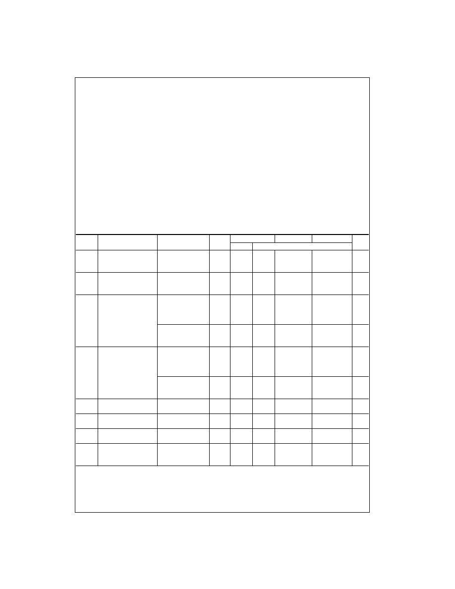
Absolute Maximum Ratings
(Note 1)
(Note 2)
Recommended Operating
Conditions
Note 1: Maximum Ratings are those values beyond which damage to the
device may occur.
Note 2: Unless otherwise specified all voltages are referenced to ground.
Note 3: Power Dissipation temperature derating -- plastic "N" package:
-
12 mW/
∞
C from 65
∞
C to 85
∞
C.
DC Electrical Characteristics
(Note 4)
Note 4: For a power supply of 5V
±
10% the worst-case output voltages (V
OH
, and V
OL
) occur for HC at 4.5V. Thus the 4.5V values should be used when
designing with this supply. Worst-case V
IH
and V
IL
occur at V
CC
=
5.5V and 4.5V respectively. (The V
IH
value at 5.5V is 3.85V.) The worst-case leakage cur-
rent (I
IN
, I
CC
, and I
OZ
) occur for CMOS at the higher voltage and so the 6.0V values should be used.
Supply Voltage (V
CC
)
-
0.5V to
+
7.0V
DC Input Voltage (V
IN
)
-
1.5V to V
CC
+
1.5V
DC Output Voltage (V
OUT
)
-
0.5V to V
CC
+
0.5V
Clamp Diode Current (I
IK
, I
OK
)
±
20 mA
DC Output Current, per pin (I
OUT
)
±
25 mA
DC V
CC
or GND Current, per pin (I
CC
)
±
50 mA
Storage Temperature Range (T
STG
)
-
65
∞
C to
+
150
∞
C
Power Dissipation (P
D
)
(Note 3)
600 mW
S.O. Package only
500 mW
Lead Temperature (T
L
)
(Soldering 10 seconds)
260
∞
C
Min
Max
Units
Supply Voltage (V
CC
)
2
6
V
DC Input or Output Voltage
(V
IN
, V
OUT
)
0
V
CC
V
Operating Temperature Range (T
A
)
-
40
+
85
∞
C
Maximum Input Rise and Fall
Time (Clear Input)
V
CC
=
2.0V
1000
ns
V
CC
=
4.5V
500
ns
V
CC
=
6.0V
400
ns
Symbol
Parameter
Conditions
V
CC
T
A
=
25
∞
C
T
A
=
-
40 to 85
∞
C T
A
=
-
55 to 125
∞
C
Units
Typ
Guaranteed Limits
V
IH
Minimum HIGH Level
2.0V
1.5
1.5
1.5
V
Input Voltage
4.5V
3.15
3.15
3.15
V
6.0V
4.2
4.2
4.2
V
V
IL
Maximum LOW Level
2.0V
0.3
0.3
0.3
V
Input Voltage
4.5V
0.9
0.9
0.9
V
6.0V
1.2
1.2
1.2
V
V
OH
Minimum HIGH Level
V
IN
=
V
IH
or V
IL
Output Voltage
|I
OUT
|
20
µ
A
2.0V
2.0
1.9
1.9
1.9
V
4.5V
4.5
4.4
4.4
4.4
V
6.0V
6.0
5.9
5.9
5.9
V
V
IN
=
V
IH
or V
IL
|I
OUT
|
4.0 mA
4.5V
4.2
3.98
3.84
3.7
V
|I
OUT
|
5.2 mA
6.0V
5.7
5.48
5.34
5.2
V
V
OL
Maximum LOW Level
V
IN
=
V
IH
or V
IL
Output Voltage
|I
OUT
|
20
µ
A
2.0V
0
0.1
0.1
0.1
V
4.5V
0
0.1
0.1
0.1
V
6.0V
0
0.1
0.1
0.1
V
V
IN
=
V
IH
or V
IL
|I
OUT
|
4.0 mA
4.5V
0.2
0.26
0.33
0.4
V
|I
OUT
|
5.2 mA
6.0V
0.2
0.26
0.33
0.4
V
I
IN
Maximum Input Current
V
IN
=
V
CC
or GND
6.0V
±
0.5
±
5.0
±
5.0
µ
A
(Pins 7, 15)
I
IN
Maximum Input Current
V
IN
=
V
CC
or GND
6.0V
±
0.1
±
1.0
±
1.0
µ
A
(all other pins)
I
CC
Maximum Quiescent Supply V
IN
=
V
CC
or GND
6.0V
8.0
80
160
µ
A
Current (standby)
I
OUT
=
0
µ
A
I
CC
Maximum Active Supply
V
IN
=
V
CC
or GND
2.0V
36
80
110
130
µ
A
Current (per monostable)
R/C
EXT
=
0.5V
CC
4.5V
0.33
1.0
1.3
1.6
mA
6.0V
0.7
2.0
2.6
3.2
mA
www.fairchildsemi.com
4
MM
74
H
C
22
1A
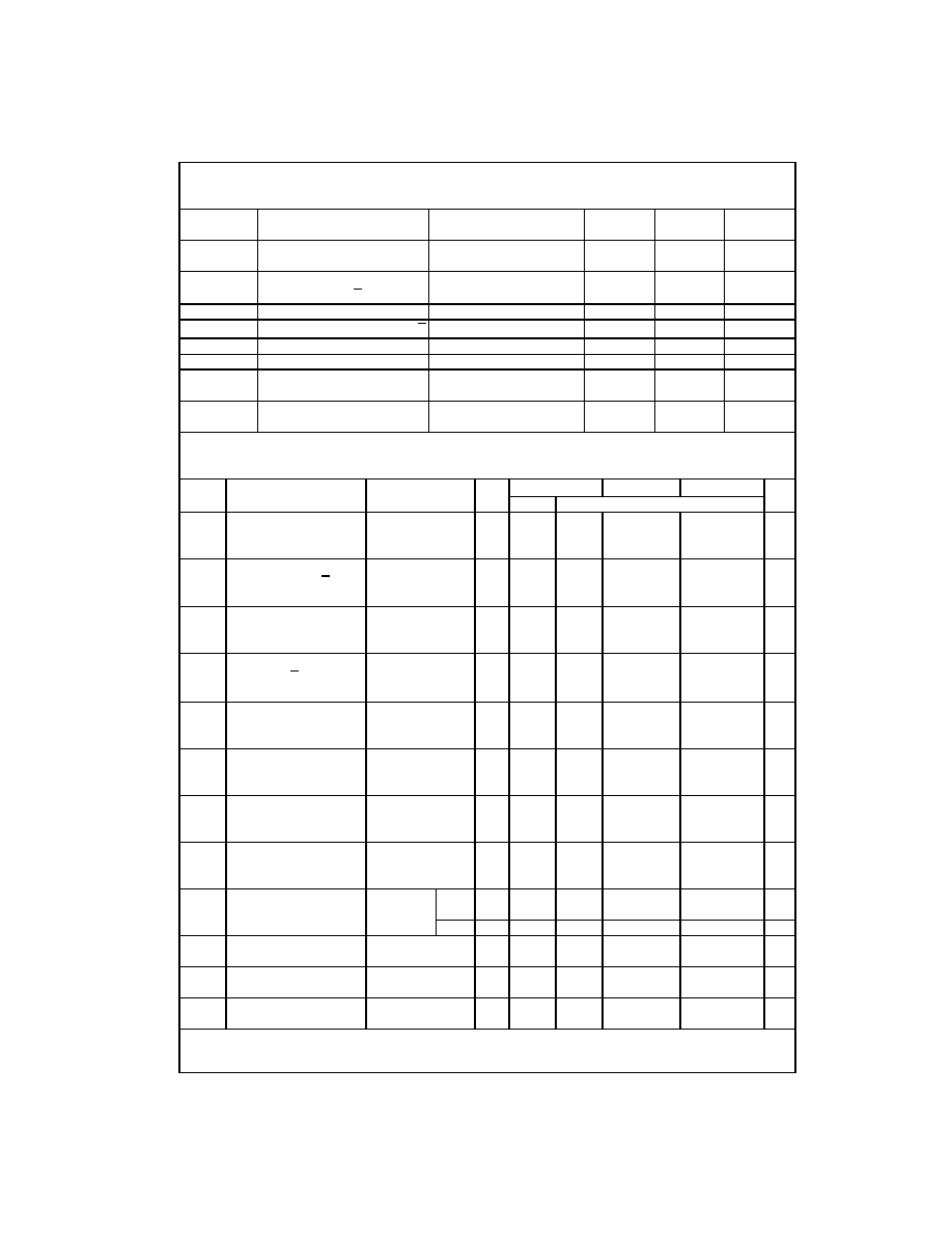
AC Electrical Characteristics
V
CC
=
5V, T
A
=
25
∞
C, C
L
=
15 pF, t
r
=
t
f
=
6 ns
AC Electrical Characteristics
C
L
=
50 pF, t
r
=
t
f
=
6 ns (unless otherwise specified)
Note 5: C
PD
determines the no load dynamic power consumption, P
D
=
C
PD
V
CC
2
f
+
I
CC
V
CC
, and the no load dynamic current consumption,
I
S
=
C
PD
V
CC
f
+
I
CC
.
Symbol
Parameter
Conditions
Typ
Guaranteed
Units
Limit
t
PLH
Maximum Trigger Propagation
22
36
ns
Delay A, B or Clear to Q
t
PHL
Maximum Trigger Propagation
25
42
ns
Delay A, B or Clear to Q
t
PHL
Maximum Propagation Delay Clear to Q
20
31
ns
t
PLH
Maximum Propagation Delay Clear to Q
22
33
ns
t
W
Minimum Pulse Width A, B or Clear
14
26
ns
t
REM
Minimum Clear Removal Time
0
ns
t
WQ(MIN)
Minimum Output Pulse Width
C
EXT
=
28 pF
400
ns
R
EXT
=
2 k
t
WQ
Output Pulse Width
C
EXT
=
1000 pF
10
µ
s
R
EXT
=
10 k
Symbol
Parameter
Conditions
V
CC
T
A
=
25
∞
C
T
A
=
-
40 to 85
∞
C T
A
=
-
55 to 125
∞
C
Units
Typ
Guaranteed Limits
t
PLH
Maximum Trigger Propagation
2.0V
77
169
194
210
ns
Delay A, B or Clear to Q
4.5V
26
42
51
57
ns
6.0V
21
32
39
44
ns
t
PHL
Maximum Trigger Propagation
2.0V
88
197
229
250
ns
Delay A, B or Clear to Q
4.5V
29
48
60
67
ns
6.0V
24
38
46
51
ns
t
PHL
Maximum Propagation
2.0V
54
114
132
143
ns
Delay Clear to Q
4.5V
23
34
41
45
ns
6.0V
19
28
33
36
ns
t
PLH
Maximum Propagation
2.0V
56
116
135
147
ns
Delay Clear to Q
4.5V
25
36
42
46
ns
6.0V
20
29
34
37
ns
t
W
Minimum Pulse Width
2.0V
57
123
144
157
ns
A, B, Clear
4.5V
17
30
37
42
ns
6.0V
12
21
27
30
ns
t
REM
Minimum Clear
2.0V
0
0
0
ns
Removal Time
4.5V
0
0
0
ns
6.0V
0
0
0
ns
t
TLH
, t
THL
Maximum Output
2.0V
30
75
95
110
ns
Rise and Fall Time
4.5V
8
15
19
22
ns
6.0V
7
13
16
19
ns
t
WQ(MIN)
Minimum Output
C
EXT
=
28 pF
2.0V
1.5
µ
s
Pulse Width
R
EXT
=
2 k
4.5V
450
ns
R
EXT
=
6 k
(V
CC
=
2V)
6.0V
380
ns
t
WQ
Output Pulse Width
C
EXT
=
0.1
µ
F
Min
5.0V
1
0.9
0.86
0.85
ms
R
EXT
=
10 k
Max
5.0V
1
1.1
1.14
1.15
ms
C
PD
Power Dissipation
87
pF
Capacitance (Note 5)
C
IN
Maximum Input
12
20
20
20
pF
Capacitance (Pins 7 & 15)
C
IN
Maximum Input
6
10
10
10
pF
Capacitance (other inputs)
5
www.fairchildsemi.com
MM74HC221A
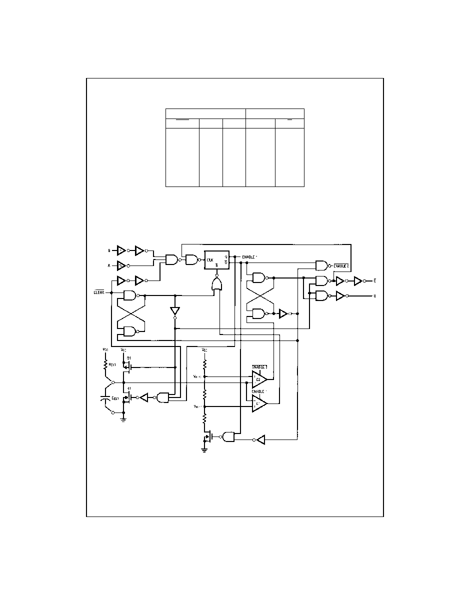
Theory of Operation
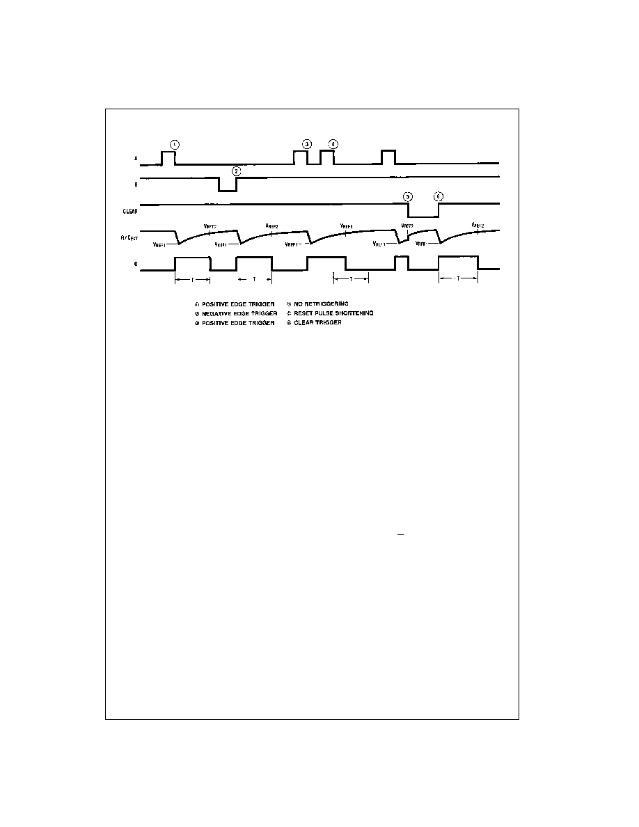
FIGURE 1.
TRIGGER OPERATION
As shown in
Figure 1 and the logic diagram before an input
trigger occurs, the monostable is in the quiescent state with
the Q output LOW, and the timing capacitor C
EXT
com-
pletely charged to V
CC
. When the trigger input A goes from
V
CC
to GND (while inputs B and clear are held to V
CC
) a
valid trigger is recognized, which turns on comparator C1
and N-channel transistor N11. At the same time the output
latch is set. With transistor N1 on, the capacitor C
EXT
rap-
idly discharges toward GND until V
REF1
is reached. At this
point the output of comparator C1 changes state and tran-
sistor N1 turns off. Comparator C1 then turns off while at
the same time comparator C2 turns on. With transistor N1
off, the capacitor C
EXT
begins to charge through the timing
resistor, R
EXT
, toward V
CC
. When the voltage across C
EXT
equals V
REF2
, comparator C2 changes state causing the
output latch to reset (Q goes LOW) while at the same time
disabling comparator C2. This ends the timing cycle with
the monostable in the quiescent state, waiting for the next
trigger.
A valid trigger is also recognized when trigger input B goes
from GND to V
CC
(while input A is at GND and input clear
is at V
CC
2). The MM74HC221 can also be triggered when
clear goes from GND to V
CC
(while A is at Gnd and B is at
V
CC
6).
It should be noted that in the quiescent state C
EXT
is fully
charged to V
CC
causing the current through resistor R
EXT
to be zero. Both comparators are "off" with the total device
current due only to reverse junction leakages. An added
feature of the MM74HC221 is that the output latch is set via
the input trigger without regard to the capacitor voltage.
Thus, propagation delay from trigger to Q is independent of
the value of C
EXT
, R
EXT
, or the duty cycle of the input
waveform.
The MM74HC221 is non-retriggerable and will ignore input
transitions on A and B until it has timed out 3 and 4.
RESET OPERATION
These one shots may be reset during the generation of the
output pulse. In the reset mode of operation, an input pulse
on clear sets the reset latch and causes the capacitor to be
fast charged to V
CC
by turning on transistor Q1 5. When
the voltage on the capacitor reaches V
REF2
, the reset latch
will clear and then be ready to accept another pulse. If the
clear input is held LOW, any trigger inputs that occur will be
inhibited and the Q and Q outputs of the output latch will
not change. Since the Q output is reset when an input low
level is detected on the Clear input, the output pulse T can
be made significantly shorter than the minimum pulse width
specification.