© 2005 Fairchild Semiconductor Corporation
DS011668
www.fairchildsemi.com
March 1994
Revised May 2005
7
4
AB
T1
6374
1
6
-Bi
t
D-T
ype Fli
p
-F
lop wit
h
3-
ST
A
T
E Output
s
74ABT16374
16-Bit D-Type Flip-Flop with 3-STATE Outputs
General Description
The ABT16374 contains sixteen non-inverting D-type flip-
flops with 3-STATE outputs and is intended for bus oriented
applications. The device is byte controlled. A buffered clock
(CP) and Output Enable (OE) are common to each byte
and can be shorted together for full 16-bit operation.
Features
s
Separate control logic for each byte
s
16-bit version of the ABT374
s
Edge-triggered D-type inputs
s
Buffered Positive edge-triggered clock
s
High impedance glitch free bus loading during entire
power up and power down cycle
s
Non-destructive hot insertion capability
s
Guaranteed latch-up protection
Ordering Code:
Devices also available in Tape and Reel. Specify by appending suffix letter "X" to the ordering code.
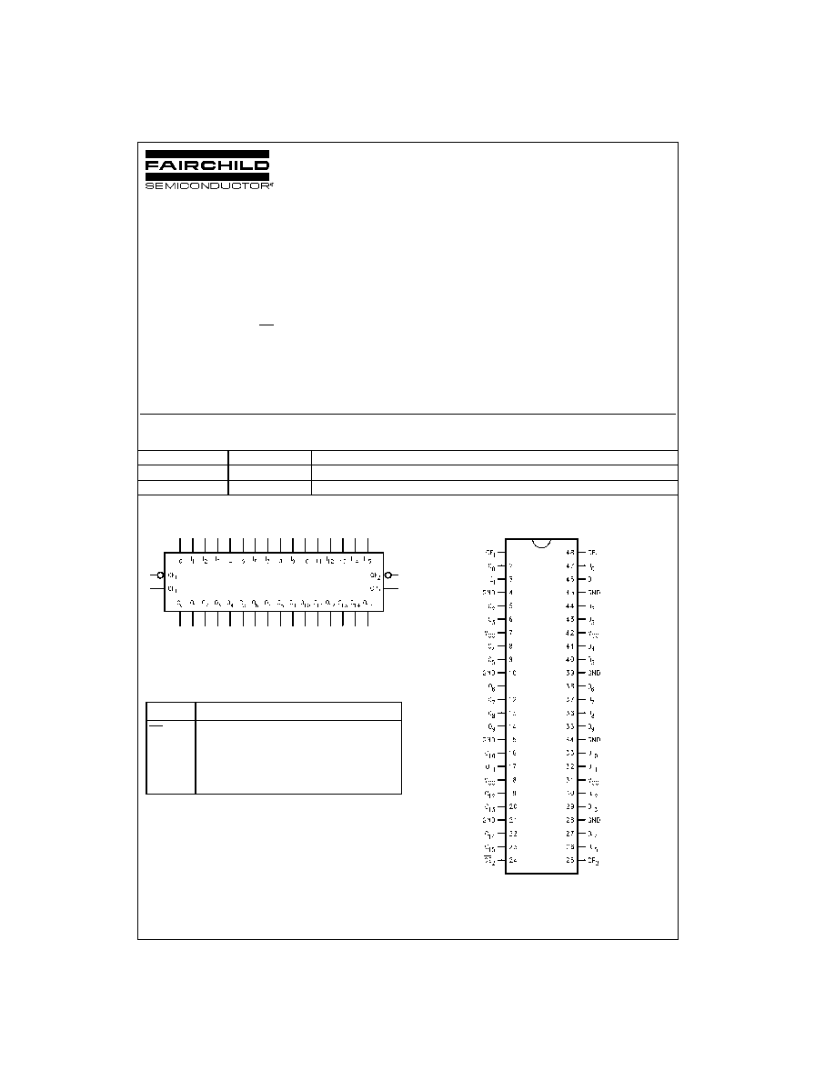
Logic Symbol
Pin Descriptions
Connection Diagram
Order Number
Package Number
Package Description
74ABT16374CSSC
MS48A
48-Lead Small Shrink Outline Package (SSOP), JEDEC MO-118, 0.300" Wide
74ABT16374CMTD
MTD48
48-Lead Thin Shrink Small Outline Package (TSSOP), JEDEC MO-153, 6.1mm Wide
Pin Name
Description
OE
n
3-STATE Output Enable Input (Active LOW)
CP
n
Clock Pulse Input (Active Rising Edge)
D
0
≠D
15
Data Inputs
O
0
≠O
15
3-STATE Outputs

www.fairchildsemi.com
2
74ABT16374
Functional Description
The ABT16374 consists of sixteen edge-triggered flip-flops
with individual D-type inputs and 3-STATE true outputs.
The device is byte controlled with each byte functioning
identically, but independent of the other. The control pins
can be shorted together to obtain full 16-bit operation. Each
byte has a buffered clock and buffered Output Enable com-
mon to all flip-flops within that byte. The description which
follows applies to each byte. Each flip-flop will store the
state of their individual D inputs that meet the setup and
hold time requirements on the LOW-to-HIGH Clock (CP
n
)
transition. With the Output Enable (OE
n
) LOW, the con-
tents of the flip-flops are available at the outputs. When
OE
n
is HIGH, the outputs go to the high impedance state.
Operation of the OE
n
input does not affect the state of the
flip-flops.
Truth Tables
H
HIGH Voltage Level
L
LOW Voltage Level
X
Immaterial
Z
High Impedance
Logic Diagrams
Byte 1 (0:7)
Byte 2 (8:15)
Inputs
Outputs
CP
1
OE
1
D
0
≠D
7
O
0
≠O
7
L
H
H
L
L
L
L
L
X
(Previous)
X
H
X
Z
Inputs
Outputs
CP
2
OE
2
D
8
≠D
15
O
8
≠O
15
L
H
H
L
L
L
L
L
X
(Previous)
X
H
X
Z

3
www.fairchildsemi.com
7
4
AB
T1
6374
Absolute Maximum Ratings
(Note 1)
Recommended Operating
Conditions
Note 1: Absolute maximum ratings are values beyond which the device
may be damaged or have its useful life impaired. Functional operation
under these conditions is not implied.
Note 2: Either voltage limit or current limit is sufficient to protect inputs.
DC Electrical Characteristics
Note 3: Guaranteed, but not tested.
Note 4: For 8-bit toggling, I
CCD
0.8 mA/MHz.
Storage Temperature
65
q
C to
150
q
C
Ambient Temperature under Bias
55
q
C to
125
q
C
Junction Temperature under Bias
55
q
C to
150
q
C
V
CC
Pin Potential to Ground Pin
0.5V to
7.0V
Input Voltage (Note 2)
0.5V to
7.0V
Input Current (Note 2)
30 mA to
5.0 mA
Voltage Applied to Any Output
in the Disabled or
Power-Off State
0.5V to 5.5V
in the HIGH State
0.5V to V
CC
Current Applied to Output
in LOW State (Max)
twice the rated I
OL
(mA)
DC Latchup Source Current:
OE Pin
350 mA
(Across Comm Operating Range)
Other Pins
500 mA
Over Voltage Latchup (I/O)
10V
Free Air Ambient Temperature
40
q
C to
85
q
C
Supply Voltage
4.5V to
5.5V
Minimum Input Edge Rate (
'
V/
'
t)
Data Input
50 mV/ns
Enable Input
20 mV/ns
Clock Input
100mV/ns
Symbol
Parameter
Min
Typ
Max
Units
V
CC
Conditions
V
IH
Input HIGH Voltage
2.0
V
Recognized HIGH Signal
V
IL
Input LOW Voltage
0.8
V
Recognized LOW Signal
V
CD
Input Clamp Diode Voltage
1.2
V
Min
I
IN
18 mA
V
OH
Output HIGH Voltage
2.5
V
Min
I
OH
3 mA
2.0
V
Min
I
OH
32 mA
V
OL
Output LOW Voltage
0.55
V
Min
I
OL
64 mA
I
IH
Input HIGH Current
1
P
A
Max
V
IN
2.7V (Note 3)
1
V
IN
V
CC
I
BVI
Input HIGH Current Breakdown Test
7
P
A
Max
V
IN
7.0V
I
IL
Input LOW Current
1
P
A
Max
V
IN
0.5V (Note 3)
1
V
IN
0.0V
V
ID
Input Leakage Test
4.75
V
0.0
I
ID
1.9
P
A
All Other Pins Grounded
I
OZH
Output Leakage Current
10
P
A
0
5.5V
V
OUT
2.7V; OE
2.0V
I
OZL
Output Leakage Current
10
P
A
0
5.5V
V
OUT
0.5V; OE
2.0V
I
OS
Output Short-Circuit Current
100
275
mA
Max
V
OUT
0.0V
I
CEX
Output HIGH Leakage Current
50
P
A
Max
V
OUT
V
CC
I
ZZ
Bus Drainage Test
100
P
A
0.0
V
OUT
5.5V; All Others V
CC
or GND
I
CCH
Power Supply Current
2.0
mA
Max
All Outputs HIGH
I
CCL
Power Supply Current
62
mA
Max
All Outputs LOW
I
CCZ
Power Supply Current
2.0
mA
Max
OE
V
CC
; All Others at V
CC
or GND
I
CCT
Additional I
CC
/Input Outputs
Enabled
2.5
mA
V
I
V
CC
2.1V
Outputs 3-STATE
2.5
mA
Max
Enable Input V
I
V
CC
2.1V
Outputs 3-STATE
2.5
mA
Data Input V
I
V
CC
2.1V
All Others at V
CC
or GND
I
CCD
Dynamic I
CC
No Load
mA/
Max
Outputs Open
(Note 3)
0.30
MHz
OE
GND, (Note 4)
One Bit Toggling, 50% Duty Cycle

www.fairchildsemi.com
4
74ABT16374
AC Electrical Characteristics
(SSOP Package)
AC Operating Requirements
Capacitance
Note 5: C
OUT
is measured at frequency f
1 MHz, per MIL-STD-883, Method 3012.
Symbol
Parameter
T
A
25
q
C
T
A
40
q
C to
85
q
C
Units
V
CC
5.0V
V
CC
4.5V to 5.5V
C
L
50 pF
C
L
50 pF
Min
Typ
Max
Min
Max
f
MAX
Maximum Clock Frequency
150
150
MHz
t
PLH
Propagation Delay
1.8
6.2
1.8
6.2
ns
t
PHL
CP to O
n
1.8
5.9
1.8
5.9
t
PZH
Output Enable Time
1.2
5.6
1.2
5.6
ns
t
PZL
1.6
5.3
1.6
5.3
t
PHZ
Output Disable Time
2.2
7.1
2.2
7.1
ns
t
PLZ
2.2
6.6
2.2
6.6
Symbol
Parameter
T
A
25
q
C
T
A
40
q
C to
85
q
C
Units
V
CC
5.0V
V
CC
4.5V to 5.5V
C
L
50 pF
C
L
50 pF
Min
Max
Min
Max
t
S
(H)
Setup Time, HIGH
1.1
1.1
ns
t
S
(L)
or LOW D
n
to CP
1.1
1.1
t
H
(H)
Hold Time, HIGH
1.3
1.3
ns
t
H
(L)
or LOW D
n
to CP
1.3
1.3
t
W
(H)
Pulse Width, CP
3.0
3.0
ns
t
W
(L)
HIGH or LOW
3.0
3.0
Symbol
Parameter
Typ
Units
Conditions
(T
A
25
q
C)
C
IN
Input Capacitance
5.0
pF
V
CC
0V
C
OUT
(Note 5)
Output Capacitance
11.0
pF
V
CC
5.0V

5
www.fairchildsemi.com
7
4
AB
T1
6374
Physical Dimensions
inches (millimeters) unless otherwise noted
48-Lead Small Shrink Outline Package (SSOP), JEDEC MO-118, 0.300" Wide
Package Number MS48A