© 1999 Fairchild Semiconductor Corporation
DS011644
www.fairchildsemi.com
October 1993
Revised November 1999
7
4
AB
T1
6646 1
6
-Bi
t
T
r
ansc
eiver
s an
d Regi
ster
s wi
th
3-
S
T
A
T
E Out
puts
74ABT16646
16-Bit Transceivers and Registers with 3-STATE Outputs
General Description
The ABT16646 consists of bus transceiver circuits with 3-
STATE, D-type flip-flops, and control circuitry arranged for
multiplexed transmission of data directly from the input bus
or from the internal registers. Data on the A or B bus will be
clocked into the registers as the appropriate clock pin goes
to a high logic level. Control OE and direction pins are pro-
vided to control the transceiver function. In the transceiver
mode, data present at the high impedance port may be
stored in either the A or the B register or in both. The select
controls can multiplex stored and real-time (transparent
mode) data. The direction control determines which bus
will receive data when the enable control OE is Active
LOW. In the isolation mode (control OE HIGH), A data may
be stored in the B register and/or B data may be stored in
the A register.
Features
s
Independent registers for A and B buses
s
Multiplexed real-time and stored data
s
A and B output sink capability of 64 mA, source
capability of 32 mA
s
Guaranteed latchup protection
s
High impedance glitch free bus loading during entire
power up and power down cycle
s
Nondestructive hot insertion capability
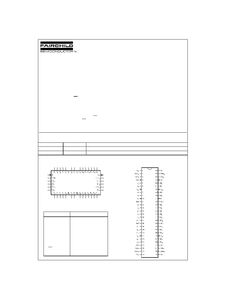
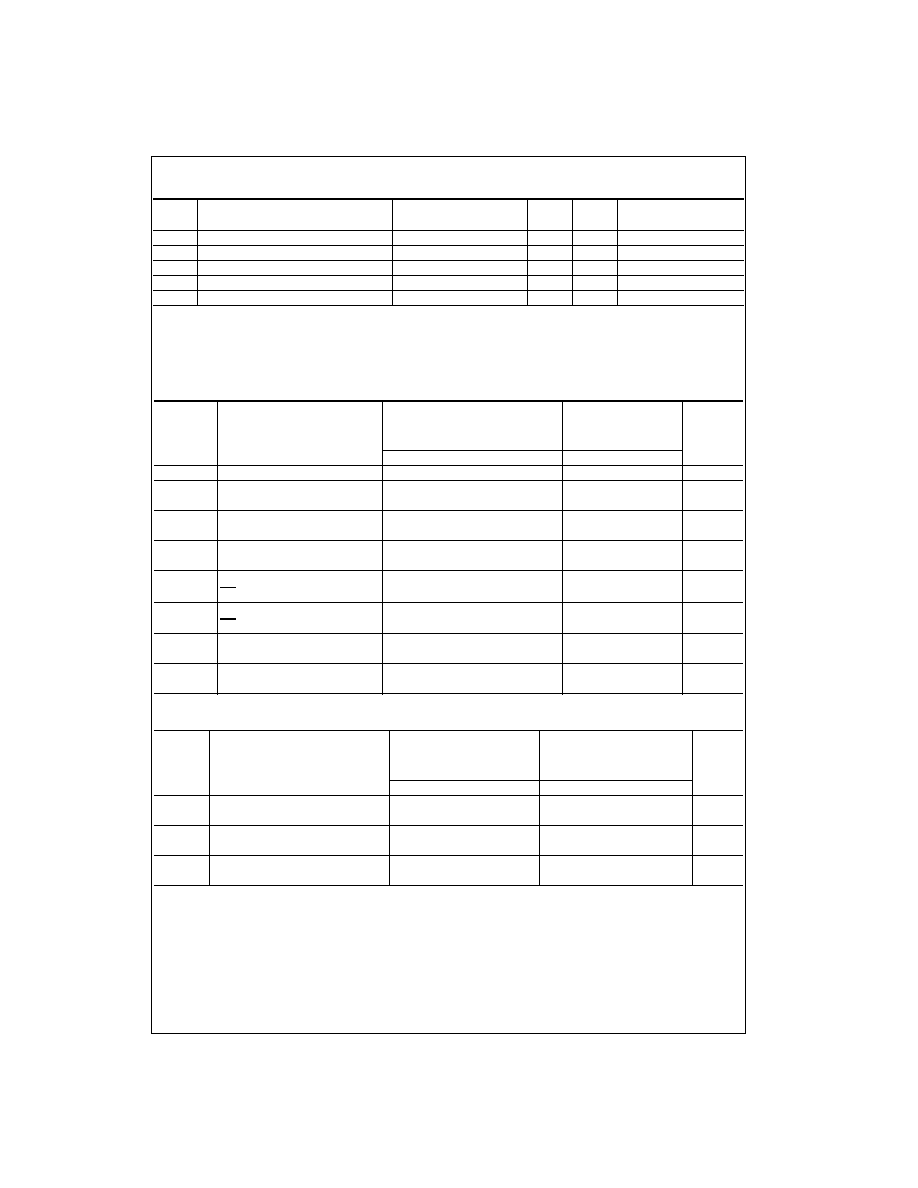
Ordering Code:
Devices also available in Tape and Reel. Specify by appending suffix letter "X" to the ordering code.
Logic Symbol
Pin Descriptions
Connection Diagram
Order Number
Package Number
Package Description
74ABT16646CSSC MS56A
56-Lead Shrink Small Outline Package (SSOP), JEDEC MO-118, 0.300" Wide
74ABT16646CMTD
MTD56
56-Lead Thin Shrink Small Outline Package (TSSOP), JEDEC MO-153, 6.1mm Wide
Pin Names
Description
A
0
≠A
15
Data Register A Inputs/
3-STATE Outputs
B
0
≠B
15
Data Register B Inputs/
3-STATE Outputs
CPAB
n
, CPBA
n
Clock Pulse Inputs
SAB
n
, SBA
n
Select Inputs
OE
n
Output Enable Input
DIR
Direction Control Input
www.fairchildsemi.com
2
74ABT16646
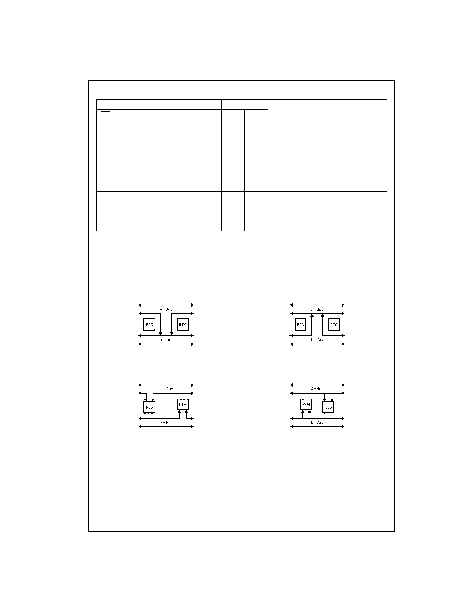
Function Table
H
=
HIGH Voltage Level
L
=
LOW Voltage Level
X
=
Immaterial
=
LOW-to-HIGH Transition
Note 1: The data output functions may be enabled or disabled by various signals at the OE and DIR inputs. Data input functions are always enabled;
i.e., data at the bus pins will be stored on every LOW-to-HIGH transition of the appropriate clock inputs. Also applies to data I/O (A and B: 8-15)
and #2 control pins.
Real Time Transfer
A-Bus to B-Bus
FIGURE 1.
Real Time Transfer
B-Bus to A-Bus
FIGURE 2.
Storage from
Bus to Register
FIGURE 3.
Transfer from
Register to Bus
FIGURE 4.
Inputs
Data I/O (Note 1)
Output Operation Mode
OE
1
DIR
1
CPAB
1
CPBA
1
SAB
1
SBA
1
A
0≠7
B
0≠7
H
X
H or L H or L
X
X
Isolation
H
X
X
X
X
Input
Input
Clock An Data into A Register
H
X
X
X
X
Clock Bn Data Into B Register
L
H
X
X
L
X
An to Bn--Real Time (Transparent Mode)
L
H
X
L
X
Input
Output Clock An Data to A Register
L
H
H or L
X
H
X
A Register to Bn (Stored Mode)
L
H
X
H
X
Clock An Data into A Register and Output to Bn
L
L
X
X
X
L
Bn to An--Real Time (Transparent Mode)
L
L
X
X
L
Output
Input
Clock Bn Data into B Register
L
L
X
H or L
X
H
B Register to An (Stored Mode)
L
L
X
X
H
Clock Bn into B Register and Output to An
3
www.fairchildsemi.com
7
4
AB
T1
6646
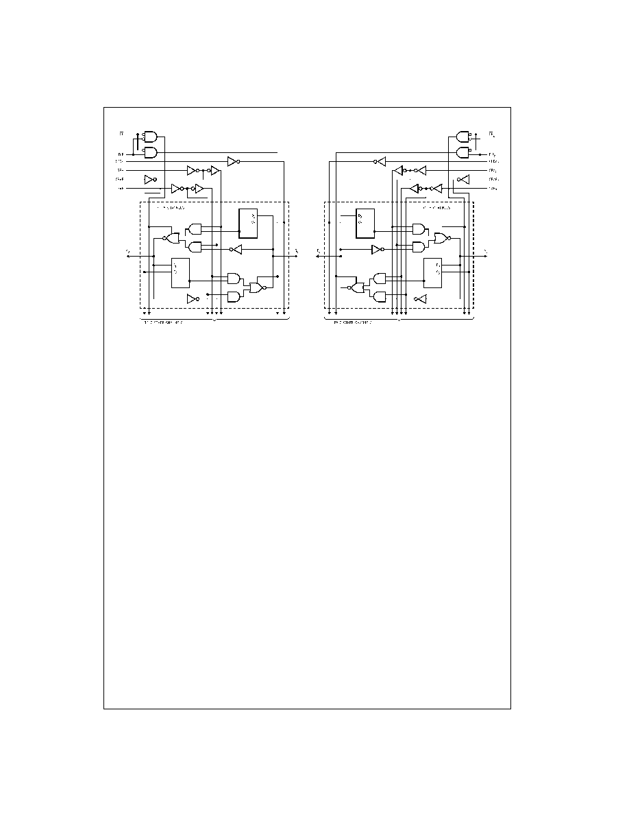
Logic Diagram
www.fairchildsemi.com
4
74ABT16646
Absolute Maximum Ratings
(Note 2)
Recommended Operating
Conditions
Note 2: Absolute maximum ratings are values beyond which the device
may be damaged or have its useful life impaired. Functional operation
under these conditions is not implied.
Note 3: Either voltage limit or current limit is sufficient to protect inputs.
DC Electrical Characteristics
Note 4: For 8-bit toggling, I
CCD
<
1.4 mA/MHz.
Note 5: Guaranteed but not tested.
Storage Temperature
-
65
∞
C to
+
150
∞
C
Ambient Temperature under Bias
-
55
∞
C to
+
125
∞
C
Junction Temperature under Bias
-
55
∞
C to
+
150
∞
C
V
CC
Pin Potential to Ground Pin
-
0.5V to
+
7.0V
Input Voltage (Note 3)
-
0.5V to
+
7.0V
Input Current (Note 3)
-
30 mA to
+
5.0 mA
Voltage Applied to Any Output
in the Disable or
Power-Off State
-
0.5V to
+
5.5V
in the HIGH State
-
0.5V to V
CC
Current Applied to Output
in LOW State (Max)
twice the rated I
OL
(mA)
DC Latchup Source Current
-
500 mA
Over Voltage Latchup (I/O)
10V
Free Air Ambient Temperature
-
40
∞
C to
+
85
∞
C
Supply Voltage
+
4.5V to
+
5.5V
Minimum Input Edge Rate (
V/
t)
Data Input
50 mV/ns
Enable Input
20 mV/ns
Clock Input
100 mV/ns
Symbol
Parameter
Min
Typ
Max
Units
V
CC
Conditions
V
IH
Input HIGH Voltage
2.0
V
Recognized HIGH Signal
V
IL
Input LOW Voltage
0.8
V
Recognized LOW Signal
V
CD
Input Clamp Diode Voltage
-
1.2
V
Min
I
IN
=
-
18 mA (Non I/O Pins)
V
OH
Output HIGH Voltage
2.5
I
OH
=
-
3 mA, (A
n
, B
n
)
2.0
I
OH
=
-
32 mA, (A
n
, B
n
)
V
OL
Output LOW Voltage
0.55
V
Min
I
OL
=
64 mA, (A
n
, B
n
)
V
ID
Input Leakage Test
4.75
V
0.0
I
ID
=
1.9
µ
A, (Non-I/O Pins)
All Other Pins Grounded
I
IH
Input HIGH Current
1
µ
A
Max
V
IN
=
2.7V (Non-I/O Pins) (Note 5)
1
V
IN
=
V
CC
(Non-I/O Pins)
I
BVI
Input HIGH Current Breakdown Test
7
µ
A
Max
V
IN
=
7.0V (Non-I/O Pins)
I
BVIT
Input HIGH Current Breakdown Test (I/O)
100
µ
A
Max
V
IN
=
5.5V (A
n
, B
n
)
I
IL
Input LOW Current
-
1
µ
A
Max
V
IN
=
0.5V (Non-I/O Pins) (Note 5)
-
1
V
IN
=
0.0V (Non-I/O Pins)
I
IH
+
I
OZH
Output Leakage Current
10
µ
A
0V≠5.5V V
OUT
=
2.7V (A
n
, B
n
); OE
=
2.0V
I
IL
+
I
OZL
Output Leakage Current
-
10
µ
A
0V≠5.5V V
OUT
=
0.5V (A
n
, B
n
); OE
=
2.0V
I
OS
Output Short-Circuit Current
-
100
-
275
mA
Max
V
OUT
=
0V (A
n
, B
n
)
I
CEX
Output HIGH Leakage Current
50
µ
A
Max
V
OUT
=
V
CC
(A
n
, B
n
)
I
ZZ
Bus Drainage Test
100
µ
A
0.0V
V
OUT
=
5.5V (A
n
, B
n
);
All Others GND
I
CCH
Power Supply Current
1.0
mA
Max
All Outputs HIGH
I
CCL
Power Supply Current
60
mA
Max
All Outputs LOW
I
CCZ
Power Supply Current
1.0
mA
Max
Outputs 3-STATE; All Others GND
I
CCT
Additional I
CC
/Input
2.5
mA
Max
V
I
=
V
CC
-
2.1V
All Other Outputs at V
CC
or GND
I
CCD
Dynamic I
CC
No Load
mA/
Max
Outputs OPEN
(Note 5)
0.23
MHz
OE, DIR, and SEL
=
GND,
Non-I/O
=
GND or V
CC
(Note 4)
One Bit toggling, 50% duty cycle
5
www.fairchildsemi.com
7
4
AB
T1
6646
DC Electrical Characteristics
(SSOP Package)
Note 6: Max number of outputs defined as (n). n
-
1 data inputs are driven 0V to 3V. One output at LOW. Guaranteed, but not tested.
Note 7: Max number of outputs defined as (n). n
-
1 data inputs are driven 0V to 3V. One output HIGH. Guaranteed, but not tested.
Note 8: Max number of data inputs (n) switching. n
-
1 inputs switching 0V to 3V. Input-under-test switching: 3V to threshold (V
ILD
), 0V to threshold (V
IHD
).
Guaranteed, but not tested.
AC Electrical Characteristics
(SSOP Package)
AC Operating Requirements
Symbol
Parameter
Min
Typ
Max
Units
V
CC
Conditions
C
L
=
50 pF, R
L
=
500
V
OLP
Quiet Output Maximum Dynamic V
OL
0.7
1.2
V
5.0
T
A
=
25
∞
C (Note 6)
V
OLV
Quiet Output Minimum Dynamic V
OL
-
1.4
-
1.0
V
5.0
T
A
=
25
∞
C (Note 6)
V
OHV
Minimum HIGH Level Dynamic Output Voltage
2.5
3.0
V
5.0
T
A
=
25
∞
(Note 7)
V
IHD
Minimum HIGH Level Dynamic Input Voltage
2.2
1.6
V
5.0
T
A
=
25
∞
C (Note 8)
V
ILD
Maximum LOW Level Dynamic Input Voltage
1.2
0.8
V
5.0
T
A
=
25
∞
C (Note 8)
Symbol
Parameter
T
A
=
+
25
∞
C
T
A
=
-
40
∞
C to
+
85
∞
C
Units
V
CC
=
+
5.0V
V
CC
=
4.5V≠5.5V
C
L
=
50 pF
C
L
=
50 pF
Min
Typ
Max
Min
Max
f
MAX
Maximum Clock Frequency
200
MHz
t
PLH
Propagation Delay
1.5
3.0
4.9
1.5
4.9
ns
t
PHL
Clock to Bus
1.5
3.4
4.9
1.5
4.9
t
PLH
Propagation Delay
1.5
2.6
4.5
1.5
4.5
ns
t
PHL
Bus to Bus
1.5
3.0
4.5
1.5
4.5
t
PLH
Propagation Delay
1.5
2.9
5.0
1.5
5.0
ns
t
PHL
SBA
n
or SAB
n
to A
n
to B
n
1.5
3.2
5.0
1.5
5.0
t
PZH
Enable Time
1.5
2.8
5.5
1.5
5.5
ns
t
PZL
OE
n
to A
n
or B
n
1.5
3.0
5.5
1.5
5.5
t
PHZ
Disable Time
1.5
3.9
6.0
1.5
6.0
ns
t
PLZ
OE
n
to A
n
or B
n
1.5
3.2
6.0
1.5
6.0
t
PZH
Enable Time
1.5
3.5
5.5
1.5
5.5
ns
t
PZL
DIR
n
to A
n
or B
n
1.5
3.2
5.5
1.5
5.5
t
PHZ
Disable Time
1.5
3.8
6.5
1.5
6.5
ns
t
PLZ
DIR
n
to A
n
or B
n
1.5
3.2
6.5
1.5
6.5
Symbol
Parameter
T
A
=
+
25
∞
C
T
A
=
-
40
∞
C to
+
85
∞
C
Units
V
CC
=
+
5.0V
V
CC
=
4.5V≠5.5V
C
L
=
50 pF
C
L
=
50 pF
Min
Max
Min
Max
t
S
(H)
Setup Time, HIGH
2.0
2.0
ns
t
S
(L)
or LOW Bus to Clock
t
H
(H)
Hold Time, HIGH
1.0
1.0
ns
t
H
(L)
or LOW Bus to Clock
t
W
(H)
Pulse Width,
3.0
3.0
ns
t
W
(L)
HIGH or LOW