November 1993
Revised January 1999
7
4
AB
T1
6952 1
6
-Bi
t
Regist
ered
T
r
anscei
ver
wit
h
3-
ST
A
T
E
Output
s
© 1999 Fairchild Semiconductor Corporation
DS011647.prf
www.fairchildsemi.com
74ABT16952
16-Bit Registered Transceiver with 3-STATE Outputs
General Description
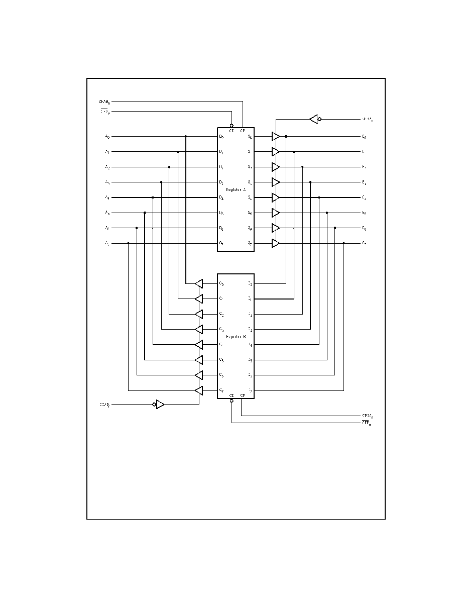
The ABT16952 is a 16-bit registered transceiver. Two 8-bit
back to back registers store data flowing in both directions
between two bidirectional buses. Separate clock, clock
enable and 3-STATE output enable signals are provided for
each register. The output pins are guaranteed to source 32
mA and to sink 64 mA.
Features
s
Separate clock, clock enable and 3-STATE output
enable provided for each register
s
A and B output sink capability of 64 mA source capability
of 32 mA
s
Guaranteed latchup protection
s
High impedance glitch free bus loading during entire
power up and power down cycle
s
Nondestructive hot insertion capability
Ordering Code:
Devices also available in Tape and Reel. Specify by appending the letter suffix "X" to the ordering code.
Pin Descriptions
Output Control
Register Function Table
(Applies to A or B Register)
H
=
HIGH Voltage Level
Z
=
HIGH Impedance
L
=
LOW Voltage Level
=
LOW-to-HIGH Transition
X
=
Immaterial
NC
=
No Change
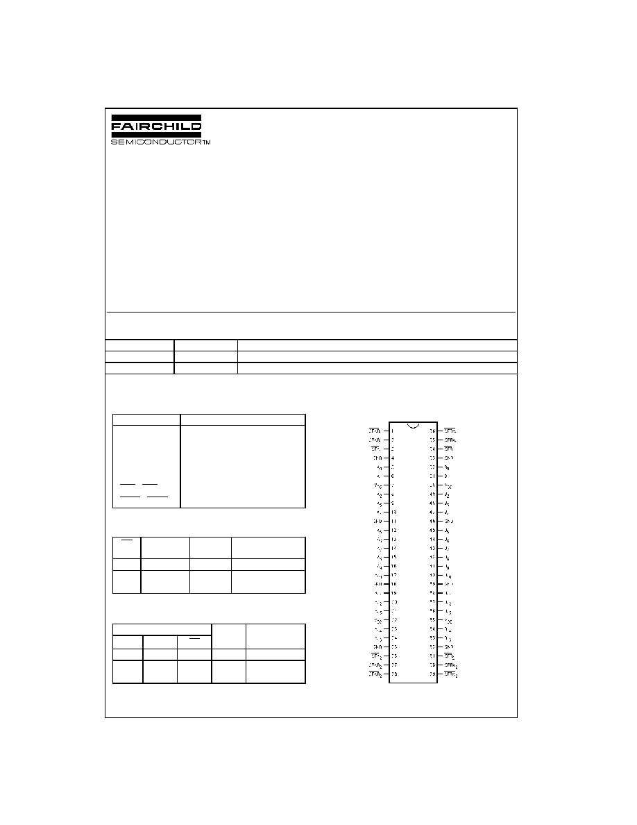
Connection Diagram
Pin Assignment for SSOP
Order Number
Package Number
Package Description
74ABT16952CSSC
MS56A
56-Lead Shrink Small Outline Package (SSOP), JEDEC MO-118, 0.300" Wide
74ABT16952CMTD
MTD56
56-Lead Thin Shrink Small Outline Package (TSSOP), JEDEC MO-153, 6.1mm Wide
Pin Names
Description
A
0
≠A
15
Data Register A Inputs/
B-Register 3-STATE Outputs
B
0
≠B
15
Data Register B Inputs/
A-Register 3-STATE Outputs
CPAB
n
, CPBA
n
Clock Pulse Inputs
CEA
n
, CEB
n
Clock Enable
OEAB
n
, OEBA
n
Output Enable Inputs
OE
Internal
Q
Output
Function
H
X
Z
Disable Outputs
L
L
L
Enable Outputs
L
H
H
Inputs
Internal
Function
D
CP
CE
Q
X
X
H
NC
Hold Data
L
L
L
Load Data
H
L
H
www.fairchildsemi.com
2
74ABT16952
Block Diagram
n for either byte 1 or byte 2

3
www.fairchildsemi.com
7
4
AB
T1
6952
Absolute Maximum Ratings
(Note 1)
Recommended Operating
Conditions
Note 1: Absolute maximum ratings are values beyond which the device
may be damaged or have its useful life impaired. Functional operation
under these conditions is not implied.
Note 2: Either voltage limit or current limit is sufficient to protect inputs.
DC Electrical Characteristics
Note 3: For 8-bit toggling, I
CCD
<
1.4 mA/MHz.
Note 4: Guaranteed, but not tested.
Storage Temperature
-
65
∞
C to
+
150
∞
C
Ambient Temperature under Bias
-
55
∞
C to
+
125
∞
C
Junction Temperature under Bias
-
55
∞
C to
+
150
∞
C
V
CC
Pin Potential to
Ground Pin
-
0.5V to
+
7.0V
Input Voltage (Note 2)
-
0.5V to
+
7.0V
Input Current (Note 2)
-
30 mA to
+
5.0 mA
Voltage Applied to Any Output
in the Disable or Power-Off State
-
0.5V to
+
5.5V
in the HIGH State
-
0.5V to V
CC
Current Applied to Output
in LOW State (Max)
twice the rated I
OL
(mA)
DC Latchup Source Current
-
500 mA
Over Voltage Latchup (I/O)
10V
Free Air Ambient Temperature
-
40
∞
C to
+
85
∞
C
Supply Voltage
+
4.5V to
+
5.5V
Minimum Input Edge Rate (
V/
t)
Data Input
50 mV/ns
Enable Input
20 mV/ns
Clock Input
100 mV/ns
Symbol
Parameter
Min
Typ
Max
Units
V
CC
Conditions
V
IH
Input HIGH Voltage
2.0
V
Recognized HIGH Signal
V
IL
Input LOW Voltage
0.8
V
Recognized LOW Signal
V
CD
Input Clamp Diode Voltage
-
1.2
V
Min
I
IN
=
-
18 mA (Non I/O Pins)
V
OH
Output HIGH Voltage
2.5
I
OH
=
-
3 mA (A
n
, B
n
)
2.0
I
OH
=
-
32 mA (A
n
, B
n
)
V
OL
Output LOW Voltage
0.55
I
OL
=
64 mA (A
n
, B
n
)
V
ID
Input Leakage Test
4.75
V
0.0
I
ID
=
1.9
µ
A (Non-I/O Pins)
All Other Pins Grounded
I
IH
Input HIGH Current
1
µ
A
Max
V
IN
=
2.7V (Non-I/O Pins) (Note 4)
1
V
IN
=
V
CC
(Non-I/O Pins)
I
BVI
Input HIGH Current
7
µ
A
Max
V
IN
=
7.0V (Non-I/O Pins)
Breakdown Test
I
BVIT
Input HIGH Current
100
µ
A
Max
V
IN
=
5.5V (A
n
, B
n
)
Breakdown Test (I/O)
I
IL
Input LOW Current
-
1
µ
A
Max
V
IN
=
0.5V (Non-I/O Pins) (Note 4)
-
1
V
IN
=
0.0V (Non-I/O Pins)
I
IH
+
I
OZH
Output Leakage Current
10
µ
A
0V≠5.5V V
OUT
=
2.7V (A
n
, B
n
);
OEA or OEB
=
2.0V
I
IL
+
I
OZL
Output Leakage Current
-
10
µ
A
0V≠5.5V V
OUT
=
0.5V (A
n
, B
n
);
OEA or OEB
=
2.0V
I
OS
Output Short-Circuit Current
-
100
-
275
mA
Max
V
OUT
=
0V (A
n
, B
n
)
I
CEX
Output HIGH Leakage Current
50
µ
A
Max
V
OUT
=
V
CC
(A
n
, B
n
)
I
ZZ
Bus Drainage Test
100
µ
A
0.0V
V
OUT
=
5.5V (A
n
, B
n
);
All Others GND
I
CCH
Power Supply Current
1.0
mA
Max
All Outputs HIGH
I
CCL
Power Supply Current
60
mA
Max
All Outputs LOW
I
CCZ
Power Supply Current
1.0
mA
Max
Outputs 3-STATE;
All Others GND
I
CCT
Additional I
CC
/Input
2.5
mA
Max
V
I
=
V
CC
-
2.1V; All Others
at V
CC
or GND
I
CCD
Dynamic I
CC
No Load
Outputs Open
(Note 4)
0.18
mA/MHz
Max
OEA or OEB
=
GND,
Non-I/O
=
GND or V
CC
One Bit toggling, 50% duty cycle
(Note 3)

www.fairchildsemi.com
4
74ABT16952
AC Electrical Characteristics
(SSOP Package)
AC Operating Requirements
Capacitance
Note 5: C
I/O
is measured at frequency f
=
1 MHz, per MIL-STD-883, Method 3012.
Symbol
Parameter
T
A
=
+
25
∞
C
T
A
=
-
40
∞
C to
+
85
∞
C
Units
V
CC
=
+
5.0V
V
CC
=
4.5V to 5.5V
C
L
=
50 pF
C
L
=
50 pF
Min
Max
Min
Max
f
max
Max Clock
200
200
MHz
Frequency
t
PLH
Propagation Delay
1.5
5.3
1.5
5.3
ns
t
PHL
CPAB
n
or CPBA
n
to
1.5
5.3
1.5
5.3
A
n
or B
n
t
PZH
Output Enable Time
1.5
5.5
1.5
5.5
ns
t
PZL
OEAB
n
or OEBA
n
to
1.5
5.5
1.5
5.5
A
n
or B
n
t
PHZ
Output Disable Time
1.5
6.0
1.5
6.0
ns
t
PLZ
OEAB
n
or OEBA
n
to
1.5
6.0
1.5
6.0
A
n
or B
n
Symbol
Parameter
T
A
=
+
25
∞
C
T
A
=
-
40
∞
C to
+
85
∞
C
Units
V
CC
=
+
5.0V
V
CC
=
4.5V to 5.5V
C
L
=
50 pF
C
L
=
50 pF
Min
Max
Min
Max
t
S
(H)
Setup Time, HIGH
2.5
2.5
ns
t
S
(L)
or LOW A
n
or B
n
2.5
2.5
to CPAB
n
or CPBA
n
t
H
(H)
Hold Time, HIGH
1.5
1.5
ns
t
H
(L)
or LOW A
n
or B
n
1.5
1.5
to CPAB
n
or CPBA
n
t
S
(H)
Setup Time, HIGH
2.5
2.5
ns
t
S
(L)
or LOW CEA
n
or CEB
n
2.5
2.5
to CPAB
n
or CPBA
n
t
H
(H)
Hold Time, HIGH
1.5
1.5
ns
t
H
(L)
or LOW CEA
n
or CEB
n
1.5
1.5
to CPAB
n
or CPBA
n
t
W
(H)
Pulse Width,
3.0
3.0
ns
t
W
(L)
HIGH or LOW
3.0
3.0
to CPAB
n
or CPBA
n
Symbol
Parameter
Typ
Units
Conditions
T
A
=
25
∞
C
C
IN
Input Capacitance
5
pF
V
CC
=
0V (Non I/O Pins)
C
I/O
(Note 5)
Output Capacitance
11
pF
V
CC
=
5.0V (A
n
, B
n
)

5
www.fairchildsemi.com
7
4
AB
T1
6952
AC Loading
*Includes jig and probe capacitance
FIGURE 1. Standard AC Test Load
FIGURE 2. Test Input Signal Levels
FIGURE 3. Input Signal Requirements
AC Waveforms
FIGURE 4. Propagation Delay Waveforms for
Inverting and Non-Inverting Functions
FIGURE 5. Propagation Delay,
Pulse Width Waveforms
FIGURE 6. 3-STATE Output HIGH
and LOW Enable and Disable Times
FIGURE 7. Setup Time, Hold Time
and Recovery Time Waveforms
Amplitude
Rep. Rate
t
W
t
r
t
f
3.0V
1 MHz
500 ns
2.5 ns
2.5 ns