© 1999 Fairchild Semiconductor Corporation
DS011550
www.fairchildsemi.com
January 1993
Revised November 1999
7
4
AB
T3
77
Oct
a
l D-T
y
pe Fl
ip-
F
lop wit
h
Cl
ock Enable
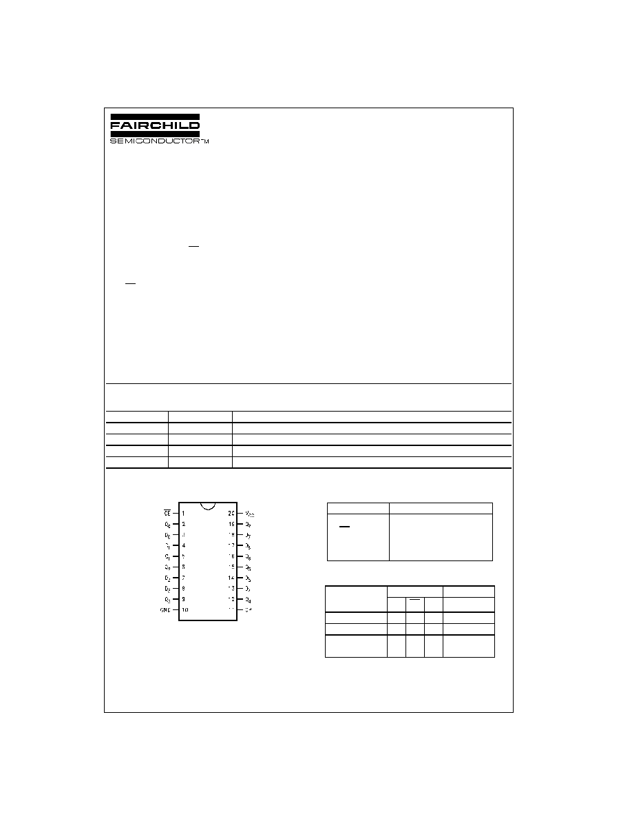
74ABT377
Octal D-Type Flip-Flop with Clock Enable
General Description
The ABT377 has eight edge-triggered, D-type flip-flops
with individual D inputs and Q outputs. The common buff-
ered Clock (CP) input loads all flip-flops simultaneously
when the Clock Enable (CE) is LOW.
The register is fully edge-triggered. The state of each D
input, one setup time before the LOW-to-HIGH clock transi-
tion, is transferred to the corresponding flip-flop's Q output.
The CE input must be stable only one setup time prior to
the LOW-to-HIGH clock transition for predictable operation.
Features
s
Clock enable for address and data synchronization
applications
s
Eight edge-triggered D-type flip-flops
s
Buffered common clock
s
See ABT273 for master reset version
s
See ABT373 for transparent latch version
s
See ABT374 for 3-STATE version
s
Output sink capability of 64 mA, source capability
of 32 mA
s
Guaranteed latchup protection
s
High impedance glitch free bus loading during entire
power up and power down cycle
s
Non-destructive hot insertion capability
s
Disable time less than enable time to avoid bus
contention
Ordering Code:
Devices also available in Tape and Reel. Specify by appending the suffix letter "X" to the ordering code.
Connection Diagram
Pin Descriptions
Truth Table
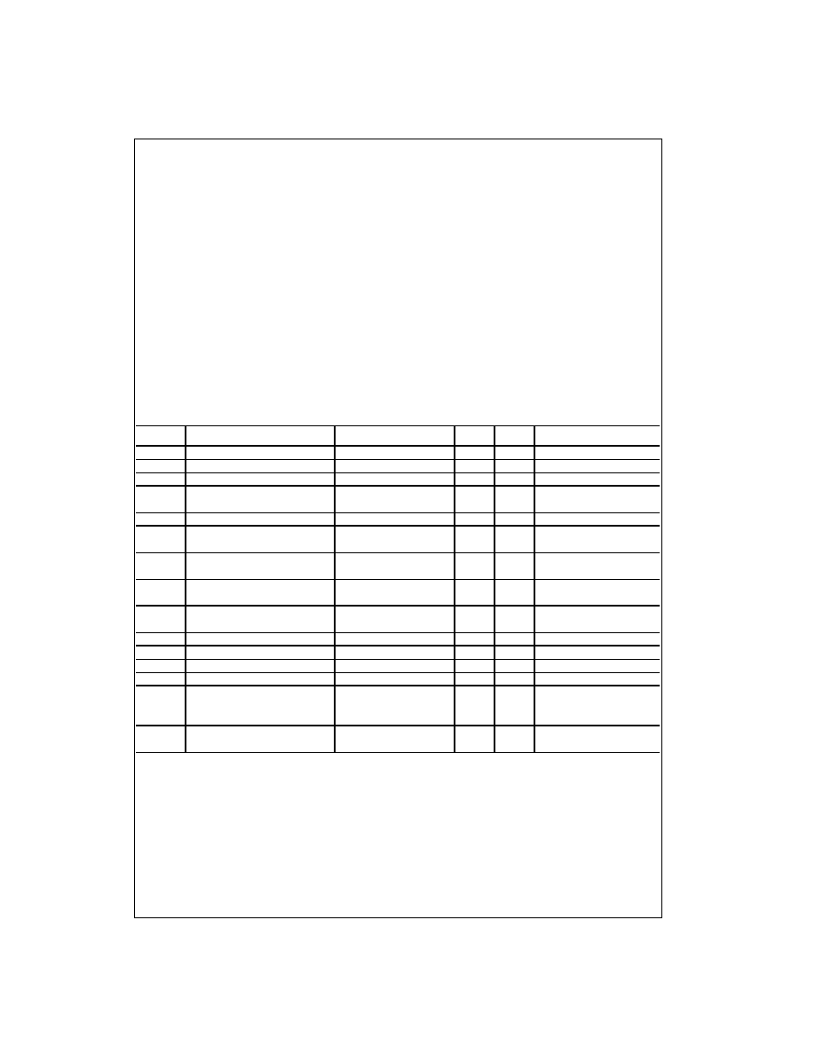
H
=
HIGH Voltage Level
L
=
LOW Voltage Level
X
=
Immaterial
=
LOW-to-HIGH Clock Transition
h
=
HIGH Voltage Level one setup time prior to the
LOW-to-HIGH Clock Transition
I
=
LOW Voltage Level one setup time prior to the
LOW-to-HIGH Clock Transition
Order Number
Package Number
Package Description
74ABT377CSC
M20B
20-Lead Small Outline Integrated Circuit (SOIC), JEDEC MS-013, 0.300" Wide Body
74ABT377CSJ
M20D
20-Lead Small Outline Package (SOP), EIAJ TYPE II, 5.3mm Wide
74ABT377CMSA
MSA20
20-Lead Shrink Small Outline Package (SSOP), EIAJ TYPE II, 5.3mm Wide
74ABT377CMTC
MTC20
20-Lead Thin Shrink Small Outline Package (TSSOP), JEDEC MO-153, 4.4mm Wide
Pin Names
Descriptions
D
0
≠D
7
Data Inputs
CE
Clock Enable (Active LOW)
CP
Clock Pulse Input
Q
0
≠Q
7
Data Outputs
Operating Mode
Inputs
Output
CP
CE
D
n
Q
n
Load "1"
I
h
H
Load "0"
I
I
L
Hold
h
X
No Change
(Do Nothing)
X
H
X
No Change
3
www.fairchildsemi.com
74
A
B
T
3
7
7
Absolute Maximum Ratings
(Note 1)
Recommended Operating
Conditions
Note 1: Absolute maximum ratings are values beyond which the device
may be damaged or have its useful life impaired. Functional operation
under these conditions is not implied.
Note 2: Either voltage limit or current limit is sufficient to protect inputs
DC Electrical Characteristics
Note 3: Guaranteed but not tested.
Note 4: For 8 bits toggling, I
CCD
<
0.5 mA/MHz.
Storage Temperature
-
65
∞
C to
+
150
∞
C
Ambient Temperature under Bias
-
55
∞
C to
+
125
∞
C
Junction Temperature under Bias
-
55
∞
C to
+
150
∞
C
V
CC
Pin Potential to Ground Pin
-
0.5V to
+
7.0V
Input Voltage (Note 2)
-
0.5V to
+
7.0V
Input Current (Note 2)
-
30 mA to
+
5.0 mA
Voltage Applied to Any Output
in the Disabled or
Power-OFF State
-
0.5V to
+
4.75V
in the HIGH State
-
0.5V to V
CC
Current Applied to Output
in LOW State (Max)
Twice the rated I
OL
(mA)
DC Latchup Source Current
-
500 mA
(Across Comm Operating Range)
Over Voltage Latchup
V
CC
+
4.5V
Free Air Ambient Temperature
-
40
∞
C to
+
85
∞
C
Supply Voltage
+
4.5V to
+
5.5V
Minimum Input Edge Rate (
V/
t)
Data Input
50 mV/ns
Enable Input
20 mV/ns
Symbol
Parameter
Min
Typ
Max
Units
V
CC
Conditions
V
IH
Input HIGH Voltage
2.0
V
Recognized HIGH Signal
V
IL
Input LOW Voltage
0.8
V
Recognized LOW Signal
V
CD
Input Clamp Diode Voltage
-
1.2
V
Min
I
IN
=
-
18 mA
V
OH
Output HIGH Voltage
2.5
V
Min
I
OH
=
-
3 mA
2.0
I
OH
=
-
32 mA
V
OL
Output LOW Voltage
0.55
V
Min
I
OL
=
64 mA
I
IH
Input HIGH Current
1
µ
A
Max
V
IN
=
2.7V (Note 3)
1
V
IN
=
V
CC
I
BVI
Input HIGH Current
7
µ
A
Max
V
IN
=
7.0V
Breakdown Test
I
IL
Input LOW Current
-
1
µ
A
Max
V
IN
=
0.5V (Note 3)
-
1
V
IN
=
0.0V
V
ID
Input Leakage Test
4.75
V
0.0
I
ID
=
1.9
µ
A
All Other Pins Grounded
I
OS
Output Short-Circuit Current
-
100
-
275
mA
Max
V
OUT
=
0.0V
I
CEX
Output HIGH Leakage Current
50
µ
A
Max
V
OUT
=
V
CC
I
CCH
Power Supply Current
50
µ
A
Max
All Outputs HIGH
I
CCL
Power Supply Current
30
mA
Max
All Outputs LOW
I
CCT
Maximum I
CC
/Input
Outputs Enabled
V
I
=
V
CC
-
2.1V
1.5
mA
Max
Data Input V
I
=
V
CC
-
2.1V
All Others at V
CC
or GND
I
CCD
Dynamic I
CC
No Load
0.3
mA/
Max
Outputs Open (Note 4)
MHz
One bit Toggling, 50% Duty Cycle

5
www.fairchildsemi.com
74
A
B
T
3
7
7
AC Loading
*Includes jig and probe capacitance
FIGURE 1. Standard AC Test Load
FIGURE 2. V
M
=
1.5V
Input Pulse Requirements
FIGURE 3. Test Input Signal Requirements
AC Waveforms
FIGURE 4. Propagation Delay Waveforms for
Inverting and Non-Inverting Functions
FIGURE 5. Propagation Delay,
Pulse Width Waveforms
FIGURE 6. 3-STATE Output HIGH
and LOW Enable and Disable Times
FIGURE 7. Setup Time, Hold Time
and Recovery Time Waveforms
Amplitude
Rep. Rate
t
W
t
r
t
f
3.0V
1 MHz
500 ns
2.5 ns
2.5 ns

