© 2005 Fairchild Semiconductor Corporation
DS011501
www.fairchildsemi.com
September 1992
Revised March 2005
7
4
AB
T5
41 Oct
a
l
Buf
f
e
r
/Li
ne
Dri
ver
w
i
t
h
3-
ST
A
T
E
O
u
tput
s
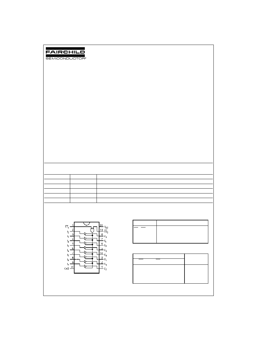
74ABT541
Octal Buffer/Line Driver with 3-STATE Outputs
General Description
The ABT541 is an octal buffer and line driver with 3-STATE
outputs designed to be employed as a memory and
address driver, clock driver, or bus-oriented transmitter/
receiver. The ABT541 is similar to the ABT244 with broad-
side pinout.
Features
s
Non-inverting buffers
s
Output sink capability of 64 mA, source capability of
32 mA
s
Guaranteed output skew
s
Guaranteed multiple output switching specifications
s
Output switching specified for both 50 pF and 250 pF
loads
s
Guaranteed simultaneous switching, noise level and
dynamic threshold performance
s
Guaranteed latchup protection
s
High impedance, glitch free bus loading during entire
power up and power down cycle
s
Nondestructive hot insertion capability
s
Flow-through pinout for ease of PC board layout
s
Disable time less than enable time to avoid bus
contention
Ordering Code:
Devices also available in Tape and Reel. Specify by appending suffix "X" to the ordering code.
Pb-Free package per JEDEC J-STD-020B.
Connection Diagram
Pin Descriptions
Truth Table
H
HIGH Voltage Level
X
Immaterial
L
LOW Voltage Level
Z
High Impedance
Order Number
Package Number
Package Description
74ABT541CSC
M20B
20-Lead Small Outline Integrated Circuit (SOIC), JEDEC MS-013, 0.300" Wide
74ABT541CSJ
M20D
Pb-Free 20-Lead Small Outline Package (SOP), EIAJ TYPE II, 5.3mm Wide
74ABT541CMSA
MSA20
20-Lead Shrink Small Outline Package (SSOP), JEDEC MO-150, 5.3mm Wide
74ABT541CMTC
MTC20
20-Lead Thin Shrink Small Outline Package (TSSOP), JEDEC MO-153, 4.4mm Wide
74ABT541CPC
N20A
20-Lead Plastic Dual-In-Line Package (PDIP), JEDEC MS-001, 0.300" Wide
Pin Names
Description
OE
1
, OE
2
Output Enable Input (Active LOW)
I
0
≠I
7
Inputs
O
0
≠O
7
Outputs
Inputs
Outputs
OE
1
OE
2
I
L
L
H
H
H
X
X
Z
X
H
X
Z
L
L
L
L
www.fairchildsemi.com
2
74ABT541
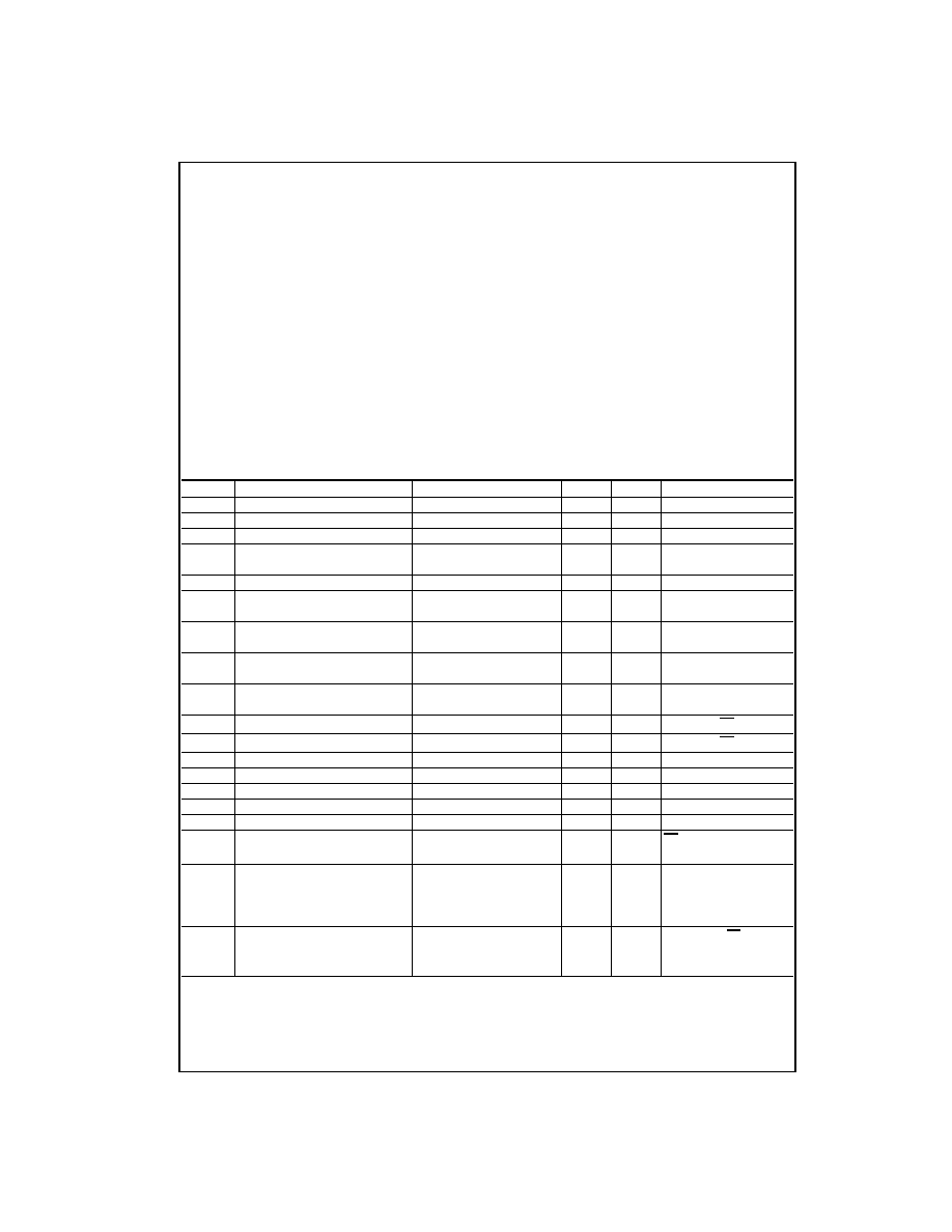
Absolute Maximum Ratings
(Note 1)
Recommended Operating
Conditions
Note 1: Absolute maximum ratings are values beyond which the device
may be damaged or have its useful life impaired. Functional operation
under these conditions is not implied.
Note 2: Either voltage limit or current limit is sufficient to protect inputs.
DC Electrical Characteristics
Note 3: For 8 bits toggling, I
CCD
0.8 mA/MHz.
Note 4: Guaranteed, but not tested.
Storage Temperature
65
q
C to
150
q
C
Ambient Temperature under Bias
55
q
C to
125
q
C
Junction Temperature under Bias
55
q
C to
150
q
C
V
CC
Pin Potential to Ground Pin
0.5V to
7.0V
Input Voltage (Note 2)
0.5V to
7.0V
Input Current (Note 2)
30 mA to
5.0 mA
Voltage Applied to Any Output
in the Disabled or
Power-Off State
0.5V to 5.5V
in the HIGH State
0.5V to V
CC
Current Applied to Output
in LOW State (Max)
twice the rated I
OL
(mA)
DC Latchup Source Current
500 mA
Over Voltage Latchup (I/O)
10V
Free Air Ambient Temperature
40
q
C to
85
q
C
Supply Voltage
4.5V to
5.5V
Minimum Input Edge Rate (
'
V/
'
t)
Data Input
50 mV/ns
Enable Input
20 mV/ns
Symbol
Parameter
Min
Typ
Max
Units
V
CC
Conditions
V
IH
Input HIGH Voltage
2.0
V
Recognized HIGH Signal
V
IL
Input LOW Voltage
0.8
V
Recognized LOW Signal
V
CD
Input Clamp Diode Voltage
1.2
V
Min
I
IN
18 mA
V
OH
Output HIGH Voltage
2.5
V
Min
I
OH
3 mA
2.0
V
Min
I
OH
32 mA
V
OL
Output LOW Voltage
0.55
V
Min
I
OL
64 mA
I
IH
Input HIGH Current
1
P
A
Max
V
IN
2.7V (Note 4)
1
V
IN
V
CC
I
BVI
Input HIGH Current
7
P
A
Max
V
IN
7.0V
Breakdown Test
I
IL
Input LOW Current
1
P
A
Max
V
IN
0.5V (Note 4)
1
V
IN
0.0V
V
ID
Input Leakage Test
4.75
V
0.0
I
ID
1.9
P
A
All Other Pins Grounded
I
OZH
Output Leakage Current
10
P
A
0
5.5V
V
OUT
2.7V; OE
n
2.0V
I
OZL
Output Leakage Current
10
P
A
0
5.5V
V
OUT
0.5V; OE
n
2.0V
I
OS
Output Short-Circuit Current
100
275
mA
Max
V
OUT
0.0V
I
CEX
Output HIGH Leakage Current
50
P
A
Max
V
OUT
V
CC
I
ZZ
Bus Drainage Test
100
P
A
0.0
V
OUT
5.5V; All Others GND
I
CCH
Power Supply Current
50
P
A
Max
All Outputs HIGH
I
CCL
Power Supply Current
30
mA
Max
All Outputs LOW
I
CCZ
Power Supply Current
50
P
A
Max
OE
n
V
CC
;
All Others at V
CC
or Ground
I
CCT
Additional I
CC
/Input
Outputs Enabled
2.5
mA
V
I
V
CC
2.1V
Outputs 3-STATE
2.5
mA
Max
Enable Input V
I
V
CC
2.1V
Outputs 3-STATE
50
P
A
Data Input V
I
V
CC
2.1V;
All Others at V
CC
or Ground
I
CCD
Dynamic I
CC
No Load
mA/
Max
Outputs Open, OE
n
GND,
(Note 4)
0.1
MHz
One Bit Toggling (Note 3),
50% Duty Cycle
3
www.fairchildsemi.com
7
4
AB
T5
41
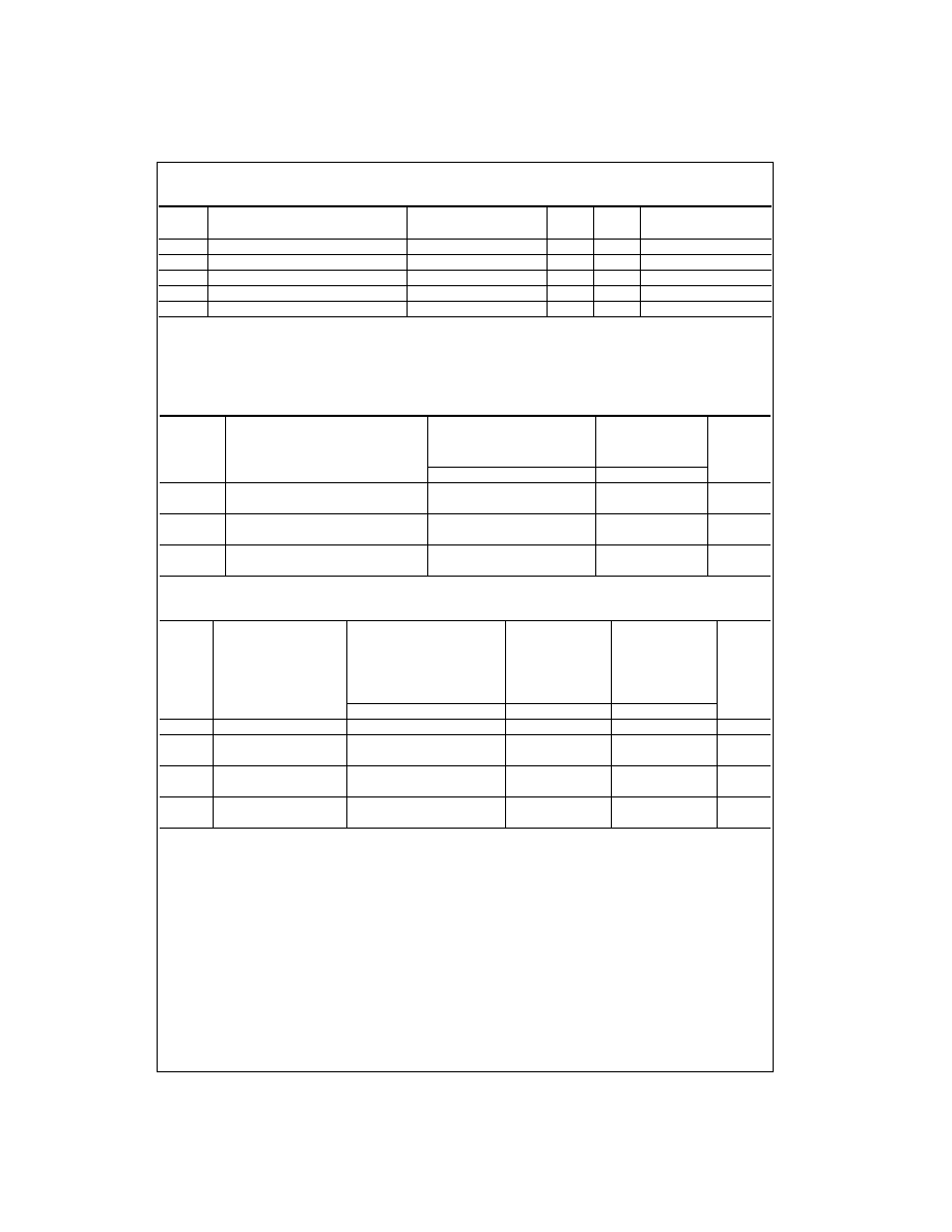
DC Electrical Characteristics
(SOIC Package)
Note 5: Max number of outputs defined as (n). n
1 data inputs are driven 0V to 3V. One output at LOW. Guaranteed, but not tested.
Note 6: Max number of outputs defined as (n). n
1 data inputs are driven 0V to 3V. One output HIGH. Guaranteed, but not tested.
Note 7: Max number of data inputs (n) switching. n
1 inputs switching 0V to 3V. Input-under-test switching: 3V to threshold (V
ILD
), 0V to threshold (V
IHD
).
Guaranteed, but not tested.
AC Electrical Characteristics
(SOIC and SSOP Package)
Extended AC Electrical Characteristics
(SOIC Package)
Note 8: This specification is guaranteed but not tested. The limits apply to propagation delays for all paths described switching in phase
(i.e., all LOW-to-HIGH, HIGH-to-LOW, etc.).
Note 9: This specification is guaranteed but not tested. The limits represent propagation delay with 250 pF load capacitors in place of the 50 pF load capac-
itors in the standard AC load. This specification pertains to single output switching only.
Note 10: This specification is guaranteed but not tested. The limits represent propagation delays for all paths described switching in phase
(i.e., all LOW-to-HIGH, HIGH-to-LOW, etc.) with 250 pF load capacitors in place of the 50 pF load capacitors in the standard AC load.
Note 11: The 3-STATE delays are dominated by the RC network (500
:
, 250 pF) on the output and have been excluded from the datasheet.
Symbol
Parameter
Min
Typ
Max
Units
V
CC
Conditions
C
L
50 pF, R
L
500
:
V
OLP
Quiet Output Maximum Dynamic V
OL
0.7
1.0
V
5.0
T
A
25
q
C (Note 5)
V
OLV
Quiet Output Minimum Dynamic V
OL
1.3
0.8
V
5.0
T
A
25
q
C (Note 5)
V
OHV
Minimum HIGH Level Dynamic Output Voltage
2.7
3.1
V
5.0
T
A
25
q
C (Note 6)
V
IHD
Minimum HIGH Level Dynamic Input Voltage
2.0
1.4
V
5.0
T
A
25
q
C (Note 7)
V
ILD
Maximum LOW Level Dynamic Input Voltage
1.1
0.6
V
5.0
T
A
25
q
C (Note 7)
Symbol
Parameter
T
A
25
q
C
T
A
40
q
C to
85
q
C
Units
V
CC
5V
V
CC
4.5V≠5.5V
C
L
50 pF
C
L
50 pF
Min
Typ
Max
Min
Max
t
PLH
Propagation Delay
1.0
2.0
3.6
1.0
3.6
ns
t
PHL
Data to Outputs
1.0
2.4
3.6
1.0
3.6
t
PZH
Output Enable Time
1.5
3.1
6.0
1.5
6.0
ns
t
PZL
1.5
3.7
6.0
1.5
6.0
t
PHZ
Output Disable Time
1.7
3.5
6.1
1.7
6.1
ns
t
PLZ
1.7
3.1
5.6
1.7
5.6
Symbol
Parameter
40
q
C to
85
q
C
T
A
40
q
C to
85
q
C
T
A
40
q
C to
85
q
C
Units
V
CC
4.5V≠5.5V
V
CC
4.5V≠5.5V
V
CC
4.5V≠5.5V
C
L
50 pF
C
L
250 pF
C
L
250 pF
8 Outputs Switching
1 Output Switching
8 Outputs Switching
(Note 8)
(Note 9)
(Note 10)
Min
Typ
Max
Min
Max
Min
Max
f
TOGGLE
Max Toggle Frequency
100
MHz
t
PLH
Propagation Delay
1.5
5.0
1.5
6.0
2.5
8.5
ns
t
PHL
Data to Outputs
1.5
5.0
1.5
6.0
2.5
8.5
t
PZH
Output Enable Time
1.5
6.5
2.5
7.5
2.5
9.5
ns
t
PZL
1.5
6.5
2.5
7.5
2.5
10.5
t
PHZ
Output Disable Time
1.0
6.1
(Note 11)
ns
t
PLZ
1.0
5.6
www.fairchildsemi.com
4
74ABT541
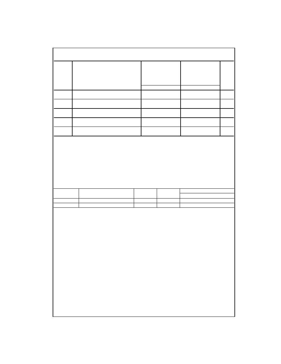
Skew
(SOIC Package)
Note 12: This specification is guaranteed but not tested. The limits apply to propagation delays for all paths described switching in phase
(i.e., all LOW-to-HIGH, HIGH-to-LOW, etc.)
Note 13: These specifications guaranteed but not tested. The limits represent propagation delays with 250 pF load capacitors in place of the 50 pF load
capacitors in the standard AC load.
Note 14: Skew is defined as the absolute value of the difference between the actual propagation delays for any two separate outputs of the same device.
The specification applies to any outputs switching HIGH-to-LOW (t
OSHL
), LOW-to-HIGH (t
OSLH
), or any combination switching LOW-to-HIGH and/or HIGH-
to-LOW (t
OST
). The specification is guaranteed but not tested.
Note 15: This describes the difference between the delay of the LOW-to-HIGH and the HIGH-to-LOW transition on the same pin. It is measured across all
the outputs (drivers) on the same chip, the worst (largest delta) number is the guaranteed specification. This specification is guaranteed but not tested.
Note 16: Propagation delay variation for a given set of conditions (i.e., temperature and V
CC
) from device to device. This specification is guaranteed but not
tested.
Capacitance
Note 17: C
OUT
is measured at frequency of f
1 MHz, per MIL-STD-883, Method 3012.
T
A
40
q
C to
85
q
C
T
A
40
q
C to
85
q
C
V
CC
4.5V≠5.5V
V
CC
4.5V≠5.5V
Symbol
Parameter
C
L
50 pF
C
L
250 pF
Units
8 Outputs Switching
8 Outputs Switching
(Note 12)
(Note 13)
Max
Max
t
OSHL
Pin to Pin Skew, HL Transitions
1.3
2.3
ns
(Note 14)
t
OSLH
Pin to Pin Skew, LH Transitions
1.0
1.8
ns
(Note 14)
t
PS
Duty Cycle, LH/HL Skew
2.0
3.5
ns
(Note 15)
t
OST
Pin to Pin Skew, LH/HL Transitions
2.0
3.5
ns
(Note 14)
t
PV
Device to Device Skew, LH/HL Transitions
2.0
3.5
ns
(Note 16)
Symbol
Parameter
Typ
Units
Conditions
T
A
25
q
C
C
IN
Input Capacitance
5.0
pF
V
CC
0.0V
C
OUT
(Note 17)
Output Capacitance
9.0
pF
V
CC
5.0V
5
www.fairchildsemi.com
7
4
AB
T5
41
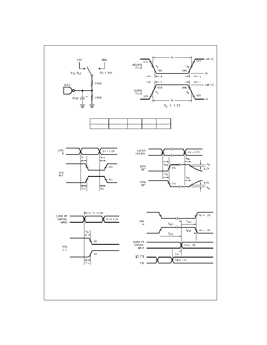
AC Loading
*Includes jig and probe capacitance
FIGURE 1. Standard AC Test Load
FIGURE 2. Test Input Signal Levels
FIGURE 3. Test Input Signal Requirements
AC Waveforms
FIGURE 4. Propagation Delay Waveforms for
Inverting and Non-Inverting Functions
FIGURE 5. Propagation Delay, Pulse Width Waveforms
FIGURE 6. 3-STATE Output HIGH and LOW
Enable and Disable Time
FIGURE 7. Setup Time, Hold Time and
Recovery Time Waveforms
Amplitude
Rep. Rate
t
W
t
r
t
f
3.0V
1 MHz
500 ns
2.5 ns
2.5 ns