 | –≠–ª–µ–∫—Ç—Ä–æ–Ω–Ω—ã–π –∫–æ–º–ø–æ–Ω–µ–Ω—Ç: 74AC11 | –°–∫–∞—á–∞—Ç—å:  PDF PDF  ZIP ZIP |

© 2000 Fairchild Semiconductor Corporation
DS009916
www.fairchildsemi.com
November 1988
Revised August 2000
7
4
AC
1
1
T
r
ipl
e
3
-
I
nput
AND Gate
74AC11
Triple 3-Input AND Gate
General Description
The AC11 contains three 3-input AND gates.
Features
s
I
CC
reduced by 50%
s
Outputs source/sink 24 mA
Ordering Code:
Device also available in Tape and Reel. Specify by appending suffix letter "X" to the ordering code.
Logic Symbol
IEEE/IEC
Connection Diagram
Pin Descriptions
FACT
is a trademark of Fairchild Semiconductor Corporation.
Order Number
Package Number
Package Description
74AC11SC
M14A
14-Lead Small Outline Integrated Circuit (SOIC), JEDEC MS-120, 0.150 Narrow
74AC11SJ
M14D
14-Lead Small Outline Package (SOP), EIAJ TYPE II, 5.3mm Wide
74AC11MTC
MTC14
14-Lead Thin Shrink Small Outline Package (TSSOP), JEDEC MO-153, 4.4mm Wide
74AC11PC
N14A
14-Lead Plastic Dual-In-Line Package (PDIP), JEDEC MS-001, 0.300 Wide
Pin Names
Description
A
n
, B
n
, C
n
Inputs
O
n
Outputs

www.fairchildsemi.com
2
74
A
C
1
1
Absolute Maximum Ratings
(Note 1)
Recommended Operating
Conditions
Note 1: Absolute maximum ratings are those values beyond which damage
to the device may occur. The databook specifications should be met, with-
out exception, to ensure that the system design is reliable over its power
supply, temperature, and output/input loading variables. Fairchild does not
recommend operation of FACT
circuits outside databook specifications.
DC Electrical Characteristics
Note 2: All outputs loaded; thresholds on input associated with output under test.
Note 3: Maximum test duration 2.0 ms, one output loaded at a time.
Note 4: I
IN
and I
CC
@ 3.0V are guaranteed to be less than or equal to the respective limit @ 5.5V V
CC
.
Supply Voltage (V
CC
)
-
0.5V to
+
7.0V
DC Input Diode Current (I
IK
)
V
I
=
-
0.5V
-
20 mA
V
I
=
V
CC
+
0.5V
+
20 mA
DC Input Voltage (V
I
)
-
0.5V to V
CC
+
0.5V
DC Output Diode Current (I
OK
)
V
O
=
-
0.5V
-
20 mA
V
O
=
V
CC
+
0.5V
+
20 mA
DC Output Voltage (V
O
)
-
0.5V to V
CC
+
0.5V
DC Output Source
or Sink Current (I
O
)
±
50 mA
DC V
CC
or Ground Current
per Output Pin (I
CC
or I
GND
)
±
50 mA
Storage Temperature (T
STG
)
-
65
∞
C to
+
150
∞
C
Junction Temperature (T
J
)
PDIP
140
∞
C
Supply Voltage (V
CC
)
2.0V to 6.0V
Input Voltage (V
I
)
0V to V
CC
Output Voltage (V
O
)
0V to V
CC
Operating Temperature (T
A
)
-
40
∞
C to
+
85
∞
C
Minimum Input Edge Rate (
V/
t)
125 mV/ns
V
IN
from 30% to 70% of V
CC
V
CC
@ 3.3V, 4.5V, 5.5V
Symbol
Parameter
V
CC
T
A
=
+
25
∞
C T
A
=
-
40
∞
C to
+
85
∞
C
Units
Conditions
(V)
Typ
Guaranteed Limits
V
IH
Minimum HIGH Level
3.0
1.5
2.1
2.1
V
OUT
=
0.1V
Input Voltage
4.5
2.25
3.15
3.15
V
or V
CC
-
0.1V
5.5
2.75
3.85
3.85
V
IL
Maximum LOW Level
3.0
1.5
0.9
0.9
V
OUT
=
0.1V
Input Voltage
4.5
2.25
1.35
1.35
V
or V
CC
-
0.1V
5.5
2.75
1.65
1.65
V
OH
Minimum HIGH Level
3.0
2.99
2.9
2.9
Output Voltage
4.5
4.49
4.4
4.4
V
I
OUT
=
-
50
µ
A
5.5
5.49
5.4
5.4
V
IN
=
V
IL
or V
IH
3.0
2.56
2.46
I
OH
=
-
12 mA
4.5
3.86
3.76
V
I
OH
=
-
24 mA
5.5
4.86
4.76
I
OH
=
-
24 mA (Note 2)
V
OL
Maximum LOW Level
3.0
0.002
0.1
0.1
Output Voltage
4.5
0.001
0.1
0.1
V
I
OUT
=
50
µ
A
5.5
0.001
0.1
0.1
V
IN
=
V
IL
or V
IH
3.0
0.36
0.44
I
OL
=
12 mA
4.5
0.36
0.44
V
I
OL
=
24 mA
5.5
0.36
0.44
I
OL
=
24 mA (Note 2)
I
IN
Maximum Input
5.5
±
0.1
±
1.0
µ
A
V
I
=
V
CC
,
(Note 4)
Leakage Current
GND
I
OLD
Minimum Dynamic
5.5
75
mA
V
OLD
=
1.65V Max
I
OHD
Output Current (Note 3)
5.5
-
75
mA
V
OHD
=
3.85V Min
I
CC
Maximum Quiescent
5.5
2.0
20.0
µ
A
V
IN
=
V
CC
(Note 4)
Supply Current
or GND

3
www.fairchildsemi.com
74
A
C
1
1
AC Electrical Characteristics
Note 5: Voltage Range 3.3 is 3.3V
±
0.3V
Voltage Range 5.0 is 5.0V
±
0.5V
Capacitance
Symbol
Parameter
V
CC
T
A
=
+
25
∞
C
T
A
=
-
40
∞
C to
+
85
∞
C
Units
(V)
C
L
=
50 pF
C
L
=
50 pF
(Note 5)
Min
Typ
Max
Min
Max
t
PLH
Propagation Delay
3.3
1.5
5.5
9.5
1.0
10.0
ns
5.0
1.5
4.0
8.0
1.0
8.5
t
PHL
Propagation Delay
3.3
1.5
5.5
8.5
1.0
9.5
ns
5.0
1.5
4.0
7.0
1.0
7.5
Symbol
Parameter
Typ
Units
Conditions
C
IN
Input Capacitance
4.5
pF
V
CC
=
OPEN
C
PD
Power Dissipation Capacitance
20.0
pF
V
CC
=
5.0V
www.fairchildsemi.com
4
74
A
C
1
1
Physical Dimensions
inches (millimeters) unless otherwise noted
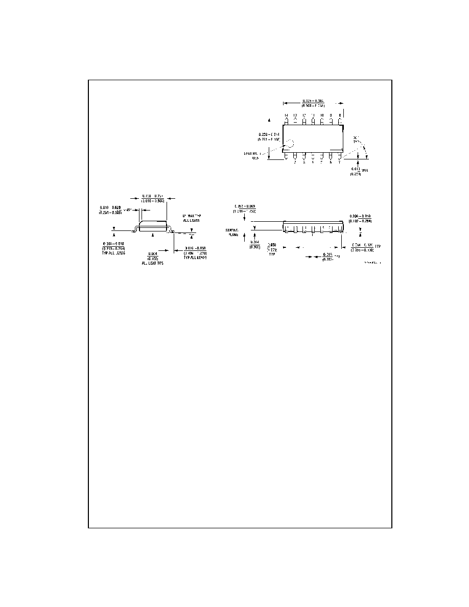
14-Lead Small Outline Integrated Circuit (SOIC), JEDEC MS-120, 0.150 Narrow
Package Number M14A

5
www.fairchildsemi.com
74
A
C
1
1
Physical Dimensions
inches (millimeters) unless otherwise noted (Continued)
14-Lead Small Outline Package (SOP), EIAJ TYPE II, 5.3mm Wide
Package Number M14D