January 1990
Revised December 1998
7
4
A
C
T899
9-
B
i
t
Lat
c
hab
le
T
r
anscei
ver
wit
h
P
a
r
i
t
y
Gener
ator
/Chec
ker
© 1999 Fairchild Semiconductor Corporation
DS010637.prf
www.fairchildsemi.com
74ACT899
9-Bit Latchable Transceiver with Parity
Generator/Checker
General Description
The ACT899 is a 9-bit to 9-bit parity transceiver with trans-
parent latches. The device can operate as a feed-through
transceiver or it can generate/check parity from the 8-bit
data busses in either direction. The ACT899 features inde-
pendent latch enables for the A-to-B direction and the B-to-
A direction, a select pin for ODD/EVEN parity, and sepa-
rate error signal output pins for checking parity.
Features
s
Latchable transceiver with output sink of 24 mA
s
Option to select generate parity and check or
"feed-through" data/parity in directions A-to-B or B-to-A
s
Independent latch enable for A-to-B and B-to-A
directions
s
Select pin for ODD/EVEN parity
s
ERRA and ERRB output pins for parity checking
s
Ability to simultaneously generate and check parity
s
May be used in system applications in place of the 280
s
May be used in system applications in place of the 657
and 373 (no need to change T/R to check parity)
Ordering Code:
Device also available in Tape and Reel. Specify by appending suffix letter "X" to the ordering code.
Logic Symbol
Connection Diagram
Pin Assignment for PCC
FACT
TM
is a trademark of Fairchild Semiconductor Corporation.
Order Number
Package Number
Package Description
74ACT899QC
V28A
28-Lead Plastic Lead Chip Carrier (PLCC), JEDEC MO-047, 0.450" Square

www.fairchildsemi.com
2
74A
CT899
Pin Descriptions
Functional Description
The ACT899 has three principal modes of operation which
are outlined below. These modes apply to both the A-to-B
and B-to-A directions.
∑ Bus A (B) communicates to Bus B (A), parity is gener-
ated and passed on to the B (A) Bus as BPAR (APAR). If
LEB (LEA) is HIGH and the Mode Select (SEL) is LOW,
the parity generated from B[0:7] (A[0:7]) can be checked
and monitored by ERRB (ERRA).
∑ Bus A (B) communicates to Bus B (A) in a feed-through
mode if SEL is HIGH. Parity is still generated and
checked as ERRA and ERRB in the feed-through mode
(can be used as an interrupt to signal a data/parity bit
error to the CPU).
∑ Independent Latch Enables (LEA and LEB) allow other
permutations of generating/checking (see Function
Table).
Function Table
H
=
HIGH Voltage Level
L
=
LOW Voltage Level
X
=
Immaterial
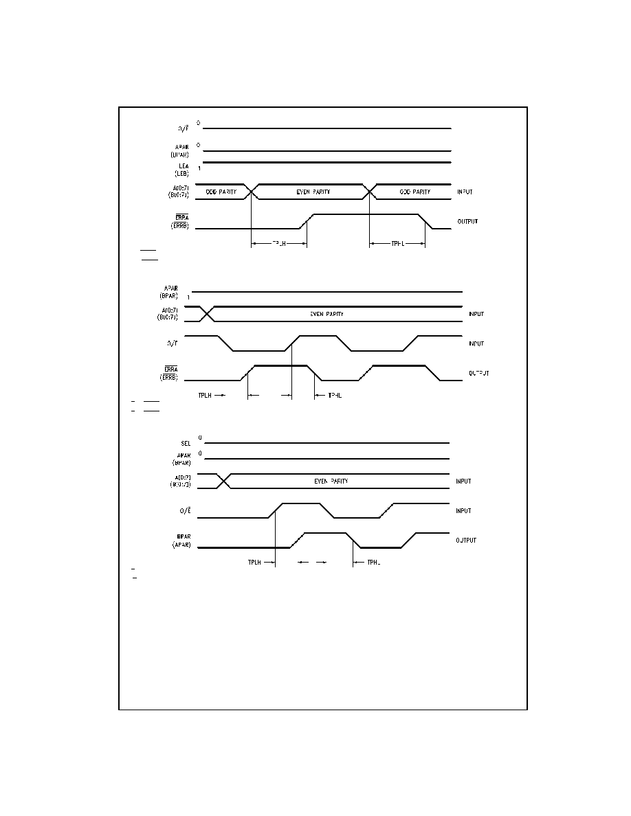
Note 1: O/E
=
ODD/EVEN
Pin Names
Description
A
0
≠A
7
A Bus Data Inputs/Data Outputs
B
0
≠B
7
B Bus Data Inputs/Data Outputs
APAR, BPAR
A and B Bus Parity Inputs
ODD/EVEN
ODD/EVEN Parity Select,
Active LOW for EVEN Parity
GBA, GAB
Output Enables for A or B Bus,
Active LOW
SEL
Select Pin for Feed-Through or Generate
Mode, LOW for Generate Mode
LEA, LEB
Latch Enables for A and B Latches,
HIGH for Transparent Mode
ERRA, ERRB
Error Signals for Checking Generated
Parity with Parity In, LOW if Error Occurs
Inputs
Operation
GAB GBA SEL LEA LEB
H
H
X
X
X
Busses A and B are 3-STATE.
H
L
L
L
H
Generates parity from B[0:7] based on O/E (Note 1). Generated parity
APAR.
Generated parity checked against BPAR and output as ERRB.
H
L
L
H
H
Generates parity from B[0:7] based on O/E. Generated parity
APAR. Generated
parity checked against BPAR and output as ERRB. Generated parity also fed back
through the A latch for generate/check as ERRA.
H
L
L
X
L
Generates parity from B latch data based on O/E. Generated parity
APAR.
Generated parity checked against latched BPAR and output as ERRB .
H
L
H
X
H
BPAR/B[0:7]
APAR/A0:7] Feed-through mode. Generated parity checked
against BPAR and output as ERRB.
H
L
H
H
H
BPAR/B[0:7]
APAR/A[0:7]
Feed-through mode. Generated parity checked against BPAR and output as ERRB.
Generated parity also fed back through the A latch for generate/check as ERRA.
L
H
L
H
L
Generates parity for A[0:7] based on O/E. Generated parity
BPAR. Generated
parity checked against APAR and output as ERRA.
L
H
L
H
H
Generates parity from A[0:7] based on O/E. Generated parity
BPAR. Generated
parity checked against APAR and output as ERRA. Generated parity also fed back
through the B latch for generate/check as ERRB.
L
H
L
L
X
Generates parity from A latch data based on O/E. Generated parity
BPAR. Gen-
erated parity checked against latched APAR and output as ERRA .
L
H
H
H
L
APAR/A[0:7]
BPAR/B[0:7]
Feed-through mode. Generated parity checked against APAR and output as ERRA.
L
H
H
H
H
APAR/A[0:7]
BPAR/B[0:7]
Feed-through mode. Generated parity checked against APAR and output as ERRA.
Generated parity also fed back through the B latch for generate/check as ERRB.