March 1990
Revised December 1998
7
4
A
C
TQ843 Quiet
Ser
i
es
TM
9-
Bit
T
r
anspar
ent Lat
c
h
wit
h
3-ST
A
T
E
Outp
uts
© 1999 Fairchild Semiconductor Corporation
DS010689.prf
www.fairchildsemi.com
74ACTQ843
Quiet Series
TM
9-Bit Transparent Latch
with 3-STATE Outputs
General Description
The ACTQ843 bus interface latch is designed to eliminate
the extra packages required to buffer existing latches and
provide extra data width for wider address/data paths. The
ACTQ843 utilizes Fairchild FACT Quiet Series
TM
technol-
ogy to guarantee quiet output switching and improved
dynamic threshold performance. FACT Quiet Series fea-
tures GTO
TM
output control and undershoot corrector in
addition to a split ground bus for superior performance.
Features
s
Guaranteed simultaneous switching noise level and
dynamic threshold performance
s
Guaranteed pin-to-pin skew AC performance
s
Inputs and outputs on opposite sides of package for
easy interface with microprocessors
s
Improved latch-up immunity
s
Outputs source/sink 24 mA
s
ACTQ843 has TTL-compatible inputs
s
Functionally and pin-compatible to AMD's AM29843
s
3-STATE outputs for bus interfacing
Ordering Code:
Device also available in Tape and Reel. Specify by appending suffix letter "X" to the ordering code.
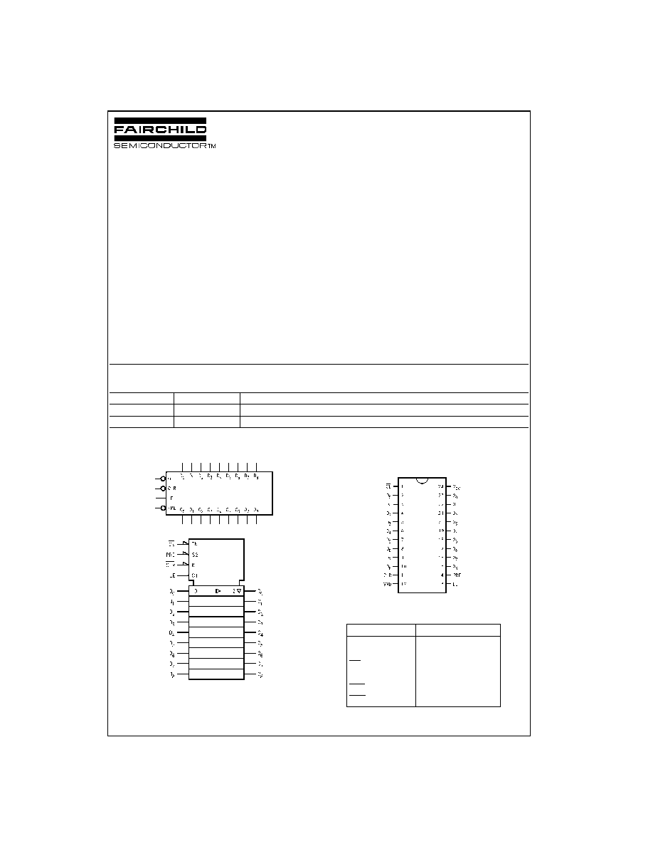
Logic Symbols
Connection Diagram
Pin Assignment for DIP and SOIC
Pin Descriptions
FACT
TM
, Quiet Series
TM
, FACT Quiet Series
TM
and GTO
TM
are trademarks of Fairchild Semiconductor Corporation.
Order Number
Package Number
Package Description
74ACTQ843SC
M24B
24-Lead Small Outline Integrated Circuit (SOIC), JEDEC MS-013, 0.300" Wide Body
74ACTQ843SPC
N24C
24-Lead Plastic Dual-In-Line Package (PDIP), JEDEC MS-100, 0.300" Wide
Pin Names
Description
D
0
≠D
8
Data Inputs
O
0
≠O
8
Data Outputs
OE
Output Enable
LE
Latch Enable
CLR
Clear
PRE
Preset

www.fairchildsemi.com
2
74A
C
T
Q
843
Functional Description
The ACTQ843 consists of nine D-type latches with 3-
STATE outputs. The flip-flops appear transparent to the
data when Latch Enable (LE) is HIGH. This allows asyn-
chronous operation, as the output transition follows the
data in transition. On the LE HIGH-to-LOW transition, the
data that meets the setup times is latched. Data appears
on the bus when the Output Enable (OE) is LOW. When
OE is HIGH, the bus output is in the high impedance state.
In addition to the LE and OE pins, the ACTQ843 has a
Clear (CLR) pin and a Preset (PRE) pin. These pins are
ideal for parity bus interfacing in high performance sys-
tems. When CLR is LOW, the outputs are LOW if OE is
LOW. When CLR is HIGH, data can be entered into the
latch. When PRE is LOW, the outputs are HIGH if OE is
LOW. Preset overrides CLR.
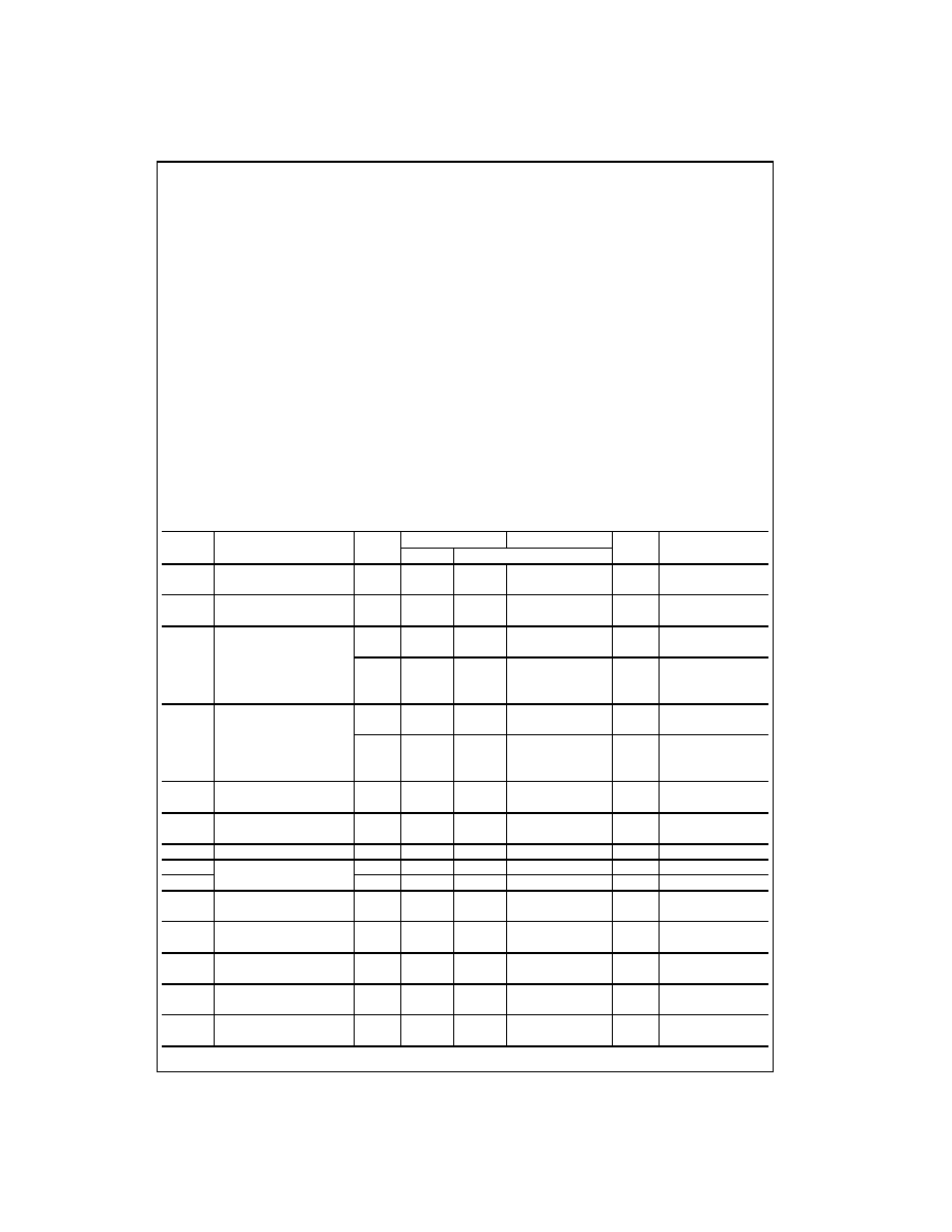
Function Table
H
=
HIGH Voltage Level
L
=
LOW Voltage Level
X
=
Immaterial
Z
=
High Impedance
NC
=
No Change
Logic Diagram
Inputs
Internal
Outputs
Function
CLR PRE
OE
LE
D
Q
O
H
H
H
H
L
L
Z
High Z
H
H
H
H
H
H
Z
High Z
H
H
H
L
X
NC
Z
Latched
H
H
L
H
L
L
L
Transparent
H
H
L
H
H
H
H
Transparent
H
H
L
L
X
NC
NC
Latched
H
L
L
X
X
H
H
Preset
L
H
L
X
X
L
L
Clear
L
L
L
X
X
H
H
Preset
L
H
H
L
X
L
Z
Clear/High Z
H
L
H
L
X
H
Z
Preset/High Z
3
www.fairchildsemi.com
7
4
A
C
TQ843
Absolute Maximum Ratings
(Note 1)
Recommended Operating
Conditions
Note 1: Absolute maximum ratings are those values beyond which damage
to the device may occur. The databook specifications should be met, with-
out exception, to ensure that the system design is reliable over its power
supply, temperature, and output/input loading variables. Fairchild does not
recommend operation of FACT
TM
circuits outside databook specifications.
DC Electrical Characteristics
Supply Voltage (V
CC
)
-
0.5V to
+
7.0V
DC Input Diode Current (I
IK
)
V
I
=
-
0.5V
-
20 mA
V
I
=
V
CC
+
0.5V
+
20 mA
DC Input Voltage (V
I
)
-
0.5V to V
CC
+
0.5V
DC Output Diode Current (I
OK
)
V
O
=
-
0.5V
-
20 mA
V
O
=
V
CC
+
0.5V
+
20 mA
DC Output Voltage (V
O
)
-
0.5V to V
CC
+
0.5V
DC Output Source
or Sink Current (I
O
)
±
50 mA
DC V
CC
or Ground Current
per Output Pin (I
CC
or I
GND
)
±
50 mA
Storage Temperature (T
STG
)
-
65
∞
C to
+
150
∞
C
DC Latch-Up Source
or Sink Current
±
300 mA
Junction Temperature (T
J
)
PDIP
140
∞
C
Supply Voltage (V
CC
)
4.5V to 5.5V
Input Voltage (V
I
)
0V to V
CC
Output Voltage (V
O
)
0V to V
CC
Operating Temperature (T
A
)
-
40
∞
C to
+
85
∞
C
Minimum Input Edge Rate
V/
t
125 mV/ns
V
IN
from 0.8V to 2.0V
V
CC
@ 4.5V, 5.5V
Symbol
Parameter
V
CC
T
A
=
+
25
∞
C
T
A
=
-
40
∞
C to
+
85
∞
C
Units
Conditions
(V)
Typ
Guaranteed Limits
V
IH
Minimum HIGH Level
4.5
1.5
2.0
2.0
V
V
OUT
=
0.1V
Input Voltage
5.5
1.5
2.0
2.0
or V
CC
-
0.1V
V
IL
Maximum LOW Level
4.5
1.5
0.8
0.8
V
V
OUT
=
0.1V
Input Voltage
5.5
1.5
0.8
0.8
or V
CC
-
0.1V
V
OH
Minimum HIGH Level
4.5
4.49
4.4
4.4
V
I
OUT
=
-
50
µ
A
Output Voltage
5.5
5.49
5.4
5.4
V
IN
=
V
IL
or V
IH
4.5
3.86
3.76
V
I
OH
=
24 mA
5.5
4.86
4.76
I
OH
=
24 mA (Note 2)
V
OL
Maximum LOW Level
4.5
0.001
0.1
0.1
V
I
OUT
=
50
µ
A
Output Voltage
5.5
0.001
0.1
0.1
V
IN
=
V
IL
or V
IH
4.5
0.36
0.44
V
I
OL
=
24 mA
5.5
0.36
0.44
I
OL
=
24 mA (Note 2)
I
IN
Maximum Input
5.5
±
0.1
±
1.0
µ
A
V
I
=
V
CC
, GND
Leakage Current
I
OZ
Maximum 3-STATE
5.5
±
0.5
±
5.0
µ
A
V
I
=
V
IL
, V
IH
Leakage Current
V
O
=
V
CC
, GND
I
CCT
Maximum I
CC
/Input
5.5
0.6
1.5
mA
V
I
=
V
CC
-
2.1V
I
OLD
Minimum Dynamic
5.5
75
mA
V
OLD
=
1.65V Max
I
OHD
Output Current (Note 3)
5.5
-
75
mA
V
OHD
=
3.85V Min
I
CC
Maximum Quiescent
5.5
8.0
80.0
µ
A
V
IN
=
V
CC
Supply Current
or GND
V
OLP
Quiet Output
5.0
1.1
1.5
V
Figure 1, Figure 2
Maximum Dynamic V
OL
(Note 4)(Note 5)
V
OLV
Quiet Output
5.0
-
0.6
-
1.2
V
Figure 1, Figure 2
Minimum Dynamic V
OL
(Note 4)(Note 5)
V
IHD
Minimum HIGH Level
5.0
1.9
2.0
V
(Note 4)(Note 6)
Dynamic Input Voltage
V
ILD
Maximum LOW Level
5.0
1.2
0.8
V
(Note 4)(Note 6)
Dynamic Input Voltage

www.fairchildsemi.com
4
74A
C
T
Q
843
DC Electrical Characteristics
(Continued)
Note 2: All outputs loaded; thresholds on input associated with output under test.
Note 3: Maximum test duration 2.0 ms, one output loaded at a time.
Note 4: DIP package.
Note 5: Max number of outputs defined as (n). Data inputs are driven 0V to 3V. One output @ GND.
Note 6: Max number of data inputs (n) switching. (n
-
1) inputs switching 0V to 3V. Input-under-test switching:
3V to threshold (V
ILD
), 0V to threshold (V
IHD
), f
=
1 MHz.
AC Electrical Characteristics
Note 7: Voltage Range 5.0 is 5.0V
±
0.5V.
Note 8: Skew is defined as the absolute value of the difference between the actual propagation delay for any two outputs within the same packaged device.
The specification applies to any outputs switching in the same direction, either HIGH to LOW (t
OSHL
) or LOW to HIGH (t
OSLH
). Parameter guaranteed by
design. Not tested.
V
CC
T
A
=
+
25
∞
C
T
A
=
-
40
∞
C to
+
85
∞
C
Symbol
Parameter
(V)
C
L
=
50 pF
C
L
=
50 pF
Units
(Note 7)
Min
Typ
Max
Min
Max
t
PLH
Propagation Delay
5.0
2.5
6.2
9.5
2.0
10.0
ns
D
n
to O
n
t
PHL
Propagation Delay
5.0
2.5
6.7
9.5
2.0
10.0
ns
D
n
to O
n
t
PLH
Propagation Delay
5.0
2.5
7.1
9.0
2.0
10.0
ns
LE to O
n
t
PHL
Propagation Delay
5.0
2.5
6.9
9.0
2.0
10.0
ns
LE to O
n
t
PLH
Propagation Delay
5.0
2.5
7.3
10.0
2.0
11.0
ns
PRE to O
n
t
PHL
Propagation Delay
5.0
2.5
7.2
11.0
2.0
12.0
ns
CLR to O
n
t
PZH
Output Enable Time
5.0
2.5
7.2
9.5
2.0
10.5
ns
OE to O
n
t
PZL
Output Enable Time
5.0
2.5
7.5
9.5
2.0
10.5
ns
OE to O
n
t
PHZ
Output Disable Time
5.0
1.5
5.0
8.0
1.0
8.5
ns
OE to O
n
t
PLZ
Output Disable Time
5.0
1.5
5.1
8.0
1.0
8.5
ns
OE to O
n
t
PHL
Propagation Delay
5.0
2.5
6.7
10.0
2.0
11.0
ns
PRE to O
n
t
PLH
Propagation Delay
5.0
2.5
7.3
11.0
2.0
12.0
ns
CLR to O
n
t
OSLH
Output to Output Skew (Note 8)
5.0
0.5
1.5
1.5
ns
t
OSHL
D
n
to O
n

5
www.fairchildsemi.com
7
4
A
C
TQ843
AC Operating Requirements
Note 9: Voltage Range 5.0 is 5.0V
±
0.5V.
Capacitance
V
CC
T
A
=
+
25
∞
C
T
A
=
-
40
∞
C to
+
85
∞
C
Symbol
Parameter
(V)
C
L
=
50 pF
C
L
=
50 pF
Units
(Note 9)
Typ
Guaranteed Minimum
t
S
Setup Time, HIGH or LOW
5.0
3.0
3.0
ns
D
n
to LE
t
H
Hold Time, HIGH or LOW
5.0
1.5
1.5
ns
D
n
to LE
t
W
LE Pulse Width, HIGH
5.0
4.0
4.0
ns
t
W
PRE Pulse Width, LOW
5.0
4.0
4.0
ns
t
W
CLR Pulse Width, LOW
5.0
4.0
4.0
ns
t
rec
PRE Recovery Time
5.0
2.0
2.0
ns
t
rec
CLR Recovery Time
5.0
2.0
2.0
ns
Symbol
Parameter
Typ
Units
Conditions
C
IN
Input Capacitance
4.5
pF
V
CC
=
OPEN
C
PD
Power Dissipation Capacitance
52
pF
V
CC
=
5.0V