 | –≠–ª–µ–∫—Ç—Ä–æ–Ω–Ω—ã–π –∫–æ–º–ø–æ–Ω–µ–Ω—Ç: 74ALS245 | –°–∫–∞—á–∞—Ç—å:  PDF PDF  ZIP ZIP |
© 2000 Fairchild Semiconductor Corporation
DS006213
www.fairchildsemi.com
September 1986
Revised February 2000
DM74ALS245A Octal
3
-
ST
A
T
E
Bus T
r
ansce
iver
DM74ALS245A
Octal 3-STATE Bus Transceiver
General Description
This advanced low power Schottky device contains 8 pairs
of 3-STATE logic elements configured as octal bus trans-
ceivers. These circuits are designed for use in memory,
microprocessor systems and in asynchronous bidirectional
data buses. Two way communication between buses is
controlled by the (DIR) input. Data transmits either from the
A bus to the B bus or from the B bus to the A bus. Both the
driver and receiver outputs can be disabled via the (G)
enable input which causes outputs to enter the high imped-
ance mode so that the buses are effectively isolated.
Features
s
Advanced oxide-isolated, ion-implanted Schottky TTL
process
s
Non-inverting logic output
s
Glitch free bus during power up and down
s
3-STATE outputs independently controlled on A and B
buses
s
Low output impedance to drive terminated transmission
lines to 133
s
Switching response specified into 500
/50 pF
s
Specified to interface with CMOS at V
OH
=
V
CC
-
2V
s
PNP inputs to reduce input loading
s
Switching specifications guaranteed over full tempera-
ture and V
CC
range
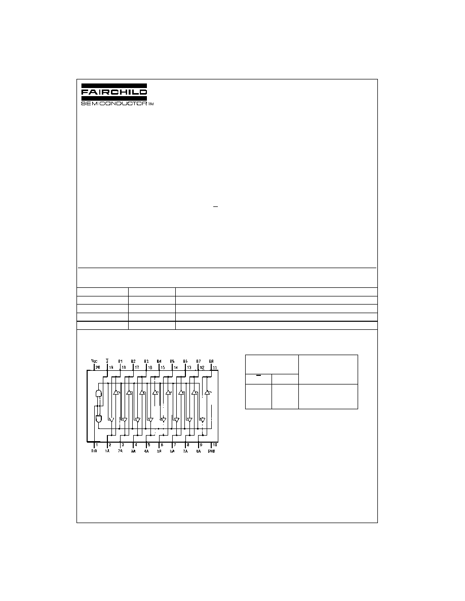
Ordering Code:
Devices also available in Tape and Reel. Specify by appending the suffix letter "X" to the ordering code.
Connection Diagram
Function Table
H
=
HIGH Logic Level
L
=
LOW Logic Level
X
=
Either HIGH or LOW Logic Level
Order Number
Package Number
Package Description
DM74ALS245AWM
M20B
20-Lead Small Outline Integrated Circuit (SOIC), JEDEC MS-013, 0.300 Wide
DM74ALS245ASJ
M20D
20-Lead Small Outline Package (SOP), EIAJ TYPE II, 5.3mm Wide
DM74ALS245AMSA
MSA20
20-Lead Shrink Small Outline Package (SSOP), EIAJ TYPE II, 5.3mm Wide
DM74ALS245AN
N20A
20-Lead Plastic Dual-In-Line Package (PDIP), JEDEC MS-001, 0.300 Wide
Control
Inputs
Operation
G
DIR
L
L
B Data to A Bus
L
H
A Data to B Bus
H
X
Hi-Z
www.fairchildsemi.com
2
DM
74ALS24
5A
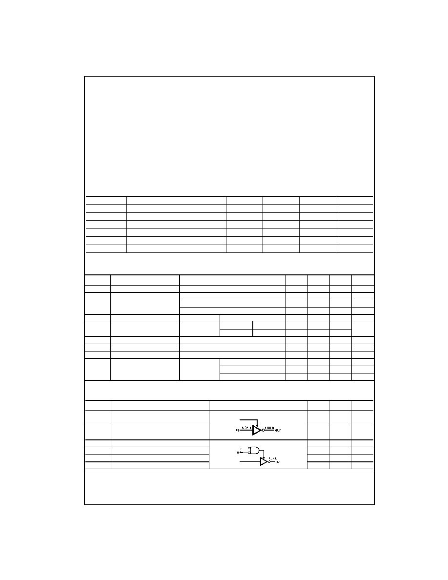
Absolute Maximum Ratings
(Note 1)
Note 1: The "Absolute Maximum Ratings" are those values beyond which
the safety of the device cannot be guaranteed. The device should not be
operated at these limits. The parametric values defined in the Electrical
Characteristics tables are not guaranteed at the absolute maximum ratings.
The "Recommended Operating Conditions" table will define the conditions
for actual device operation.
Recommended Operating Conditions
Electrical Characteristics
over recommended operating free air temperature range. All typical values are measured at V
CC
=
5V, T
A
=
25
∞
C.
Switching Characteristics
(Note 2)
over recommended operating free air temperature range
Note 2: Switching characteristic conditions are V
CC
=
4.5V to 5.5V, R
L
=
500
, C
L
=
50 pF.
Supply Voltage
7V
Input Voltage
Control Inputs
7V
I/O Ports
5.5V
Operating Free Air Temperature Range
0
∞
C to
+
70
∞
C
Storage Temperature Range
-
65
∞
C to
+
150
∞
C
Typical
JA
N Package
53.0
∞
C/W
M Package
72.0
∞
C/W
Symbol
Parameter
Min
Typ
Max
Units
V
CC
Supply Voltage
4.5
5
5.5
V
V
IH
HIGH Level Input Voltage
2
V
V
IL
LOW Level Input Voltage
0.8
V
I
OH
HIGH Level Output Current
-
15
mA
I
OL
LOW Level Output Current
24
mA
T
A
Operating Free Air Temperature
0
70
∞
C
Symbol
Parameter
Conditions
Min
Typ
Max
Units
V
IK
Input Clamp Voltage
V
CC
=
4.5V, I
IN
=
-
18 mA
-
1.5
V
V
OH
HIGH Level
V
CC
=
4.5V, I
OH
=
-
3 mA
2.4
3.2
V
Output Voltage
V
CC
=
4.5V, I
OH
=
Max
2
2.3
V
I
OH
=
-
0.4 mA, V
CC
=
4.5V to 5.5V
V
CC
-
2
V
V
OL
LOW Level Output Voltage
V
CC
=
4.5V
I
OL
=
24 mA
0.35
0.5
V
I
I
Input Current at Maximum
V
CC
=
5.5V
V
IN
=
7V
Control Inputs
0.1
mA
Input Voltage
V
IN
=
5.5V
A or B Ports
0.1
I
IH
HIGH Level Input Current
V
CC
=
5.5V, V
IN
=
2.7V
20
µ
A
I
IL
LOW Level Input Current
V
CC
=
5.5V, V
IN
=
0.4V
-
0.1
mA
I
O
Output Drive Current
V
CC
=
5.5V, V
OUT
=
2.25V
-
30
-
112
mA
I
CC
Supply Current
V
CC
=
5.5V
Outputs HIGH
30
45
mA
Outputs LOW
36
55
mA
3-STATE
38
58
mA
Symbol
Parameter
Circuit Configuration
Min
Max
Units
t
PLH
Propagation Delay Time
3
10
ns
LOW-to-HIGH Level Output
t
PHL
Propagation Delay Time
3
10
ns
HIGH-to-LOW Level Output
t
PZL
Output Enable Time to LOW Level
5
20
ns
t
PZH
Output Enable Time to HIGH Level
5
20
ns
t
PLZ
Output Disable Time from LOW Level
4
15
ns
t
PHZ
Output Disable Time from HIGH Level
2
10
ns
3
www.fairchildsemi.com
DM74ALS245A
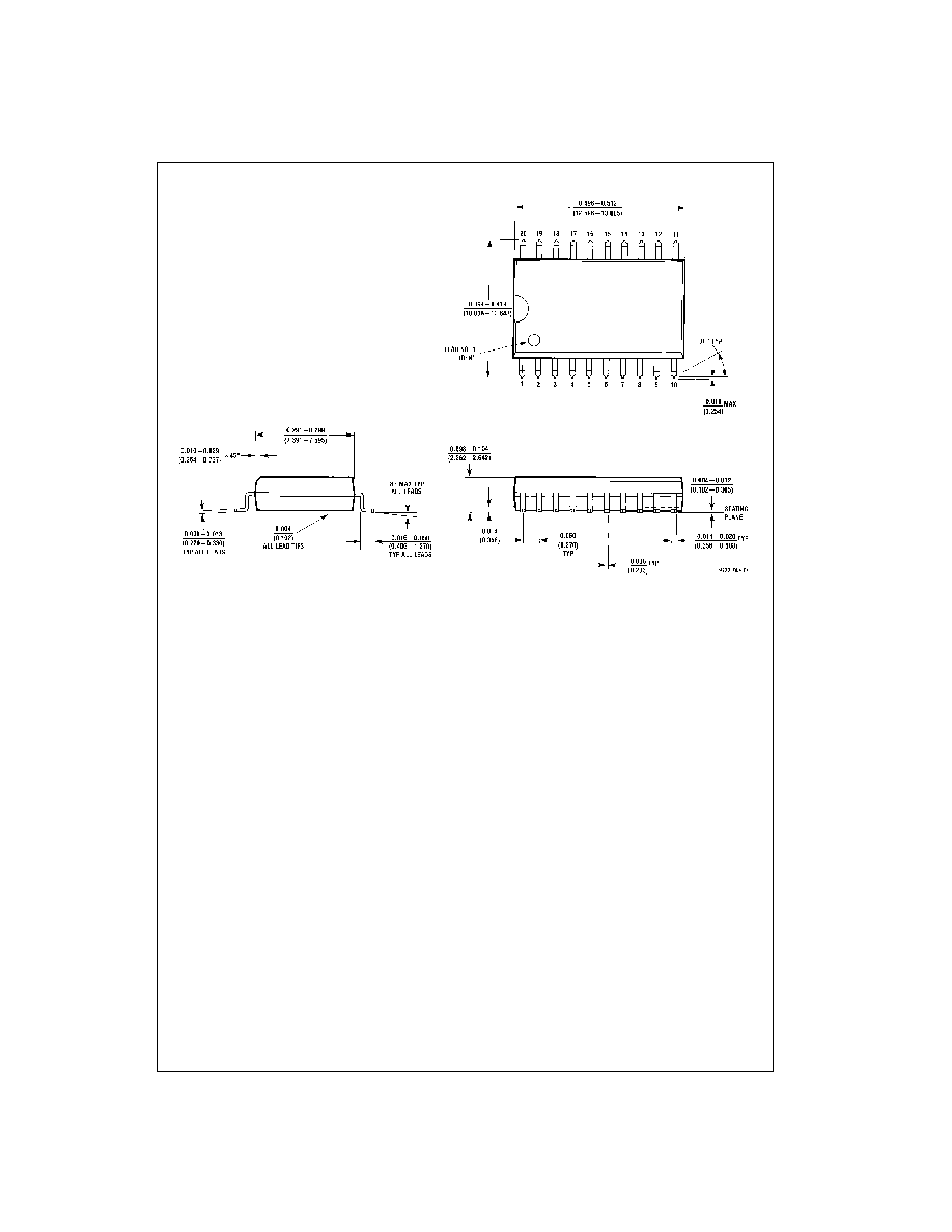
Physical Dimensions
inches (millimeters) unless otherwise noted
20-Lead Small Outline Integrated Circuit (SOIC), JEDEC MS-013, 0.300 Wide
Package Number M20B
www.fairchildsemi.com
4
DM
74ALS24
5A
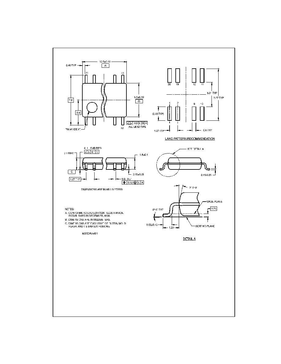
Physical Dimensions
inches (millimeters) unless otherwise noted (Continued)
20-Lead Small Outline Package (SOP), EIAJ TYPE II, 5.3mm Wide
Package Number M20D

5
www.fairchildsemi.com
DM74ALS245A
Physical Dimensions
inches (millimeters) unless otherwise noted (Continued)
20-Lead Shrink Small Outline Package (SSOP), EIAJ TYPE II, 5.3mm Wide
Package Number MSA20

www.fairchildsemi.com
6
DM74ALS245A Octal
3-
ST
A
T
E Bus T
r
anscei
ver
Physical Dimensions
inches (millimeters) unless otherwise noted (Continued)
20-Lead Plastic Dual-In-Line Package (PDIP), JEDEC MS-001, 0.300 Wide
Package Number N20A
Fairchild does not assume any responsibility for use of any circuitry described, no circuit patent licenses are implied and
Fairchild reserves the right at any time without notice to change said circuitry and specifications.
LIFE SUPPORT POLICY
FAIRCHILD'S PRODUCTS ARE NOT AUTHORIZED FOR USE AS CRITICAL COMPONENTS IN LIFE SUPPORT
DEVICES OR SYSTEMS WITHOUT THE EXPRESS WRITTEN APPROVAL OF THE PRESIDENT OF FAIRCHILD
SEMICONDUCTOR CORPORATION. As used herein:
1. Life support devices or systems are devices or systems
which, (a) are intended for surgical implant into the
body, or (b) support or sustain life, and (c) whose failure
to perform when properly used in accordance with
instructions for use provided in the labeling, can be rea-
sonably expected to result in a significant injury to the
user.
2. A critical component in any component of a life support
device or system whose failure to perform can be rea-
sonably expected to cause the failure of the life support
device or system, or to affect its safety or effectiveness.
www.fairchildsemi.com