 | –≠–ª–µ–∫—Ç—Ä–æ–Ω–Ω—ã–π –∫–æ–º–ø–æ–Ω–µ–Ω—Ç: 74F413PC | –°–∫–∞—á–∞—Ç—å:  PDF PDF  ZIP ZIP |

© 1999 Fairchild Semiconductor Corporation
DS009541
www.fairchildsemi.com
April 1988
Revised August 1999
7
4F413 64
x 4 Fir
s
t-
In Fir
s
t-
Out Buff
er Mem
o
r
y
wi
th Paral
l
el
I/
O
74F413
64 x 4 First-In First-Out Buffer Memory with Parallel I/O
General Description
The F413 is an expandable fall-through type high-speed
First-In First-Out (FIFO) buffer memory organized as 64
words by four bits. The 4-bit input and output registers
record and transmit, respectively, asynchronous data in
parallel form. Control pins on the input and output allow for
handshaking and expansion. The 4-bit wide, 62-bit deep
fall-through stack has self-contained control logic.
Features
s
Separate input and output clocks
s
Parallel input and output
s
Expandable without external logic
s
15 MHz data rate
s
Supply current 160 mA max
s
Available in SOIC, (300 mil only)
Ordering Code:
Devices also available in Tape and Reel. Specify by appending the suffix letter "X" to the ordering code.
Logic Symbol
Connection Diagram
Unit Loading/Fan Out
Order Number
Package Number
Package Description
74F413PC
N16E
16-Lead Plastic Dual-In-Line Package (PDIP), JEDEC MS-001, 0.300 Wide
Pin Names
Description
U.L.
Input I
IH
/I
IL
HIGH/LOW
Output I
OH
/I
OL
D
0
≠D
3
Data Inputs
1.0/0.667
20
µ
A/
-
0.4 mA
O
0
≠O
3
Data Outputs
50/13.3
-
1 mA/8 mA
IR
Input Ready
1.0/0.667
20
µ
A/
-
0.4 mA
SI
Shift In
1.0/0.667
20
µ
A/
-
0.4 mA
SO
Shift Out
1.0/0.667
20
µ
A/
-
0.4 mA
OR
Output Ready
1.0/0.667
20
µ
A/
-
0.4 mA
MR
Master Reset
1.0/0.667
20
µ
A/
-
0.4 mA

www.fairchildsemi.com
2
74F413
Functional Description
Data Input-- Data is entered into the FIFO on D
0
≠D
3
inputs. To enter data the Input Ready (IR) should be HIGH,
indicating that the first location is ready to accept data.
Data then present at the four data inputs is entered into the
first location when the Shift In (SI) is brought HIGH. An SI
HIGH signal causes the IR to go LOW. Data remains at the
first location until SI is brought LOW. When SI is brought
LOW and the FIFO is not full, IR will go HIGH, indicating
that more room is available. Simultaneously, data will prop-
agate to the second location and continue shifting until it
reaches the output stage or a full location. If the memory is
full, IR will remain LOW.
Data Transfer-- Once data is entered into the second cell,
the transfer of any full cell to the adjacent (downstream)
empty cell is automatic, activated by an on-chip control.
Thus data will stack up at the end of the device while empty
locations will "bubble" to the front. The t
PT
parameter
defines the time required for the first data to travel from
input to the output of a previously empty device.
Data Output-- Data is read from the O
0
≠O
3
outputs.
When data is shifted to the output stage, Output Ready
(OR) goes HIGH, indicating the presence of valid data.
When the OR is HIGH, data may be shifted out by bringing
the Shift Out (SO) HIGH. A HIGH signal at SO causes the
OR to go LOW. Valid data is maintained while the SO is
HIGH. When SO is brought LOW, the upstream data, pro-
vided that stage has valid data, is shifted to the output
stage. When new valid data is shifted to the output stage,
OR goes HIGH. If the FIFO is emptied, OR stays LOW, and
O
0
≠O
3
remains as before, i.e., data does not change if
FIFO is empty.
Input Ready and Output Ready-- may also be used as
status signals indicating that the FIFO is completely full
(Input Ready stays LOW for at least t
PT
) or completely
empty (Output Ready stays LOW for at least t
PT
).
Block Diagram

3
www.fairchildsemi.com
7
4F413
Absolute Maximum Ratings
(Note 1)
Recommended Operating
Conditions
Note 1: Absolute maximum ratings are values beyond which the device
may be damaged or have its useful life impaired. Functional operation
under these conditions is not implied.
Note 2: Either voltage limit or current limit is sufficient to protect inputs.
DC Electrical Characteristics
Storage Temperature
-
65
∞
C to
+
150
∞
C
Ambient Temperature under Bias
-
55
∞
C to
+
125
∞
C
Junction Temperature under Bias
-
55
∞
C to
+
150
∞
C
V
CC
Pin Potential to Ground Pin
-
0.5V to
+
7.0V
Input Voltage (Note 2)
-
0.5V to
+
7.0V
Input Current (Note 2)
-
30 mA to
+
5.0 mA
Voltage Applied to Output
in HIGH State (with V
CC
=
0V)
Standard Output
-
0.5V to V
CC
3-STATE Output
-
0.5V to
+
5.5V
Current Applied to Output
in LOW State (Max)
twice the rated I
OL
(mA)
Free Air Ambient Temperature
0
∞
C to
+
70
∞
C
Supply Voltage
+
4.5V to
+
5.5V
Symbol
Parameter
Min
Typ
Max
Units
V
CC
Conditions
V
IH
Input HIGH Voltage
2.0
V
Recognized as a HIGH Signal
V
IL
Input LOW Voltage
0.8
V
Recognized as a LOW Signal
V
CD
Input Clamp Diode Voltage
-
1.5
V
Min
I
IN
=
-
18 mA
V
OH
Output HIGH
10% V
CC
2.4
V
Min
I
OH
=
-
1 mA
Voltage
5% V
CC
2.7
I
OH
=
-
1 mA
V
OL
Output LOW Voltage
10% V
CC
0.5
V
Min
I
OL
=
8 mA
I
IH
Input HIGH Current
5.0
µ
A
Max
V
IN
=
2.7V
I
BVI
Input HIGH Current
7.0
µ
A
Max
V
IN
=
7.0V
Breakdown Test
I
CEX
Output HIGH Leakage Current
50
µ
A
Max
V
OUT
=
V
CC
V
ID
Input Leakage
4.75
V
0.0
I
ID
=
1.9
µ
A
Test
All Other Pins Grounded
I
OD
Output Leakage
3.75
µ
A
0.0
V
IOD
=
150 mV
Circuit Current
All Other Pins Grounded
I
IL
Input LOW Current
-
0.4
mA
Max
V
IN
=
0.5V
I
OS
Output Short-Circuit Current
-
20
-
130
mA
Max
V
OUT
=
0V
I
CCH
Power Supply Current
115
160
mA
Max
V
O
=
HIGH

www.fairchildsemi.com
4
74F413
AC Electrical Characteristics
AC Operating Requirements
Symbol
Parameter
T
A
=
+
25
∞
C
T
A
=
-
55
∞
C to
+
125
∞
C
T
A
=
0
∞
to
+
70
∞
C
Units
V
CC
=
+
5.0V
V
CC
=
+
5.0V
V
CC
=
+
5.0V
C
L
=
50 pF
C
L
=
50 pF
C
L
=
50 pF
Min
Typ
Max
Min
Max
Min
Max
f
MAX
Shift In Rate
10
8.0
10
MHz
f
MAX
Shift Out Rate
10
8.0
10
MHz
t
PLH
Propagation Delay
1.5
44.0
1.5
50.0
1.5
48.0
ns
t
PHL
Shift In to IR
1.5
31.0
1.5
37.0
1.5
35.0
t
PLH
Propagation Delay
1.5
52.0
1.5
57.0
1.5
55.0
ns
t
PHL
Shift Out to OR
1.5
31.0
1.5
37.0
1.5
35.0
t
PLH
Propagation Delay
1.5
46.0
1.5
52.0
1.5
50.0
ns
t
PHL
Output Data Delay
1.5
34.0
1.5
39.0
1.5
37.0
t
PLH
Propagation Delay
1.5
27.0
1.5
33.0
1.5
31.0
ns
Master Reset to IR
t
PLH
Propagation Delay
1.5
30.0
1.5
34.0
1.5
32.0
ns
Master Reset to OR
Symbol
Parameter
T
A
=
+
25
∞
C
T
A
=
-
55
∞
C to
+
125
∞
C
T
A
=
0
∞
to
+
70
∞
C
Units
V
CC
=
+
5.0V
V
CC
=
+
5.0V
V
CC
=
+
5.0V
Min
Max
Min
Max
Min
Max
t
S
(H)
Setup Time, HIGH or LOW
1.0
1.0
1.0
ns
t
S
(L)
D
n
to SI
1.0
1.0
1.0
t
H
(H)
Hold Time, HIGH or LOW
10.0
10.0
10.0
t
H
(L)
D
n
to SI
10.0
10.0
10.0
t
W
(H)
Shift In Pulse Width
5.0
5.0
5.0
ns
t
W
(L)
HIGH or LOW
10.0
10.0
10.0
t
W
(H)
Shift Out Pulse Width
7.5
8.5
7.5
t
W
(L)
HIGH or LOW
10.0
10.0
10.0
t
W
(H)
Input Ready Pulse Width,
7.5
8.5
7.5
ns
HIGH
t
W
(L)
Output Ready Pulse Width,
5.0
5.0
5.0
ns
LOW
t
W
(L)
Master Reset Pulse Width,
10.0
10.0
10.0
ns
LOW
t
REC
Recovery Time, MR to SI
32.0
35.0
35.0
ns
t
PT
Data Throughput Time
0.9
1.0
1.0
µ
s
5
www.fairchildsemi.com
7
4F413 64
x 4 Fir
s
t-
In Fir
s
t-
Out Buff
er Mem
o
r
y
wi
th Paral
l
el
I/
O
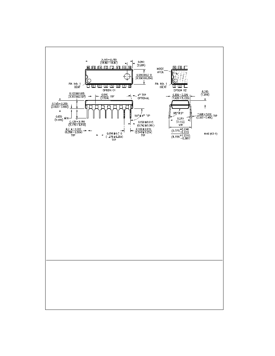
Physical Dimensions
inches (millimeters) unless otherwise noted
16-Lead Plastic Dual-In-Line Package (PDIP), JEDEC MS-001, 0.300 Wide
Package Number N16E
Fairchild does not assume any responsibility for use of any circuitry described, no circuit patent licenses are implied and
Fairchild reserves the right at any time without notice to change said circuitry and specifications.
LIFE SUPPORT POLICY
FAIRCHILD'S PRODUCTS ARE NOT AUTHORIZED FOR USE AS CRITICAL COMPONENTS IN LIFE SUPPORT
DEVICES OR SYSTEMS WITHOUT THE EXPRESS WRITTEN APPROVAL OF THE PRESIDENT OF FAIRCHILD
SEMICONDUCTOR CORPORATION. As used herein:
1. Life support devices or systems are devices or systems
which, (a) are intended for surgical implant into the
body, or (b) support or sustain life, and (c) whose failure
to perform when properly used in accordance with
instructions for use provided in the labeling, can be rea-
sonably expected to result in a significant injury to the
user.
2. A critical component in any component of a life support
device or system whose failure to perform can be rea-
sonably expected to cause the failure of the life support
device or system, or to affect its safety or effectiveness.
www.fairchildsemi.com