© 1999 Fairchild Semiconductor Corporation
DS010652
www.fairchildsemi.com
March 1990
Revised August 1999
7
4F794 8-Bi
t Regist
er wit
h
Readba
ck
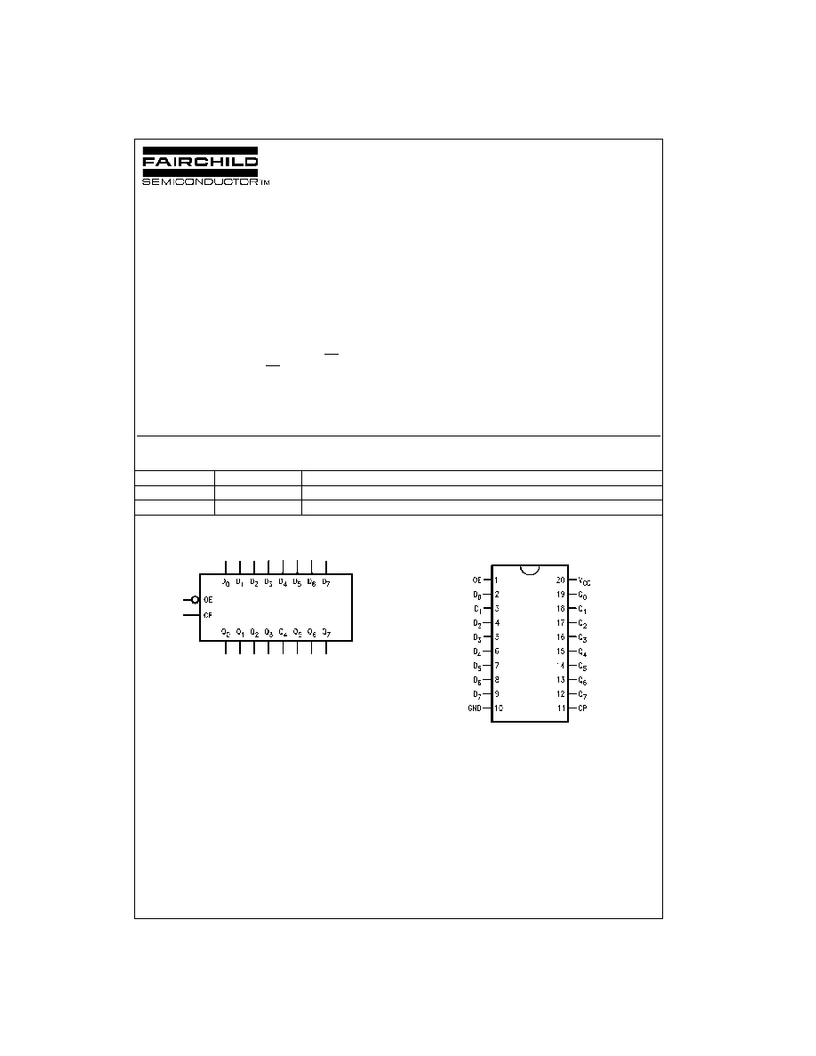
74F794
8-Bit Register with Readback
General Description
The 74F794 is an 8-bit register with readback capability
designed to store data as well as read the register informa-
tion back onto the data bus. The I/O bus (D bus) has 3-
STATE outputs. Current sinking capability is 64 mA on both
the D and Q busses.
Data is loaded into the registers on the LOW-to-HIGH tran-
sition of the clock (CP). The output enable (OE) is used to
enable data on D
0
≠D
7
. When OE is LOW, the output of the
registers is enabled on D
0
≠D
7
, enabling D as an output
bus. When OE is HIGH, D
0
≠D
7
are inputs to the registers
configuring D as an input bus.
Features
s
3-STATE outputs on the I/O port
s
D and Q output sink capability of 64 mA
s
Functionally and pin equivalent to the 74LS794
Ordering Code:
Devices also available in Tape and Reel. Specify by appending the suffix letter "X" to the ordering code.
Logic Symbol
Connection Diagram
Order Number
Package Number
Package Description
74F794SC
M20B
20-Lead Small Outline Integrated Circuit (SOIC), JEDEC MS-013, 0.300 Wide
74F794PC
N20A
20-Lead Plastic Dual-In-Line Package (PDIP), JEDEC MS-001, 0.300 Wide
3
www.fairchildsemi.com
7
4F794
Absolute Maximum Ratings
(Note 2)
Recommended Operating
Conditions
Note 2: Absolute maximum ratings are values beyond which the device
may be damaged or have its useful life impaired. Functional operation
under these conditions is not implied.
Note 3: In this case the output of the register is clocked to the inputs and
the overall Q output is unchanged at Q
n
.
Note 4: Either voltage limit or current limit is sufficient to protect inputs.
DC Electrical Characteristics
over Operating Temperature Range unless otherwise specified
Storage Temperature
-
65
∞
C to
+
150
∞
C
Ambient Temperature under Bias
-
55
∞
to
+
125
∞
C
Junction Temperature under Bias
-
55
∞
C to
+
150
∞
C
V
CC
Pin Potential to Ground Pin
-
0.5V to
+
7.0V
Input Voltage (Note 3)
-
0.5V to
+
7.0V
Input Current (Note 3)
-
30 mA to
+
5.0 mA
ESD Last Passing Voltage (Min)
4000V
Voltage Applied to Output
In HIGH State (with V
CC
=
0V)
Standard Output
-
0.5V to V
CC
3-STATE Output
-
0.5V to
+
5.5V
Current Applied to Output
in LOW State (Max)
Twice the Rated I
OL
(mA)
Free Air Ambient Temperature
0
∞
C to 70
∞
C
Supply Voltage
+
4.5V to
+
5.5V
Symbol
Parameter
Min
Typ
Max
Units
V
CC
Conditions
V
IH
Input HIGH Voltage
2.0
V
Recognized as a HIGH Signal
V
IL
Input LOW Voltage
0.8
V
Recognized as a LOW Signal
V
CD
Input Clamp
-
1.2
V
Min
I
IN
=
-
18 mA
Diode Voltage
V
OH
Output HIGH
2.4
2.8
V
Min
I
OH
=
-
3 mA
Voltage
2.0
2.44
I
OH
=
-
15 mA
V
OL
Output LOW
0.45
0.55
V
Min
I
OL
=
64 mA
Voltage
I
IH
Input HIGH
5.0
µ
A
Max
V
IN
=
2.7V
Current
I
BVI
Input HIGH Current
7.0
µ
A
Max
V
IN
=
7.0V (OE, CP)
Breakdown Test
I
BVIT
Input HIGH Current
0.5
mA
Max
V
IN
=
5.5V (D
n
)
Breakdown (I/O)
I
CEX
Output HIGH
50
µ
A
Max
V
OUT
=
V
CC
Leakage Current
V
ID
Input Leakage
4.75
V
0.0
I
ID
=
1.9
µ
A
Test
All Other Pins Grounded
I
OD
Output Leakage
3.75
µ
A
0.0
V
IOD
=
150 mV
Circuit Current
All Other Pins Grounded
I
IL
Input LOW
-
0.6
mA
Max
V
IN
=
0.5V
Current
(OE, CP)
I
OS
Output Short-
-
100
-
225
mA
Max
V
OUT
=
0V
Circuit Current
I
IH
+
Output Leakage Current
70
µ
A
Max
V
OUT
=
2.7V
I
OZH
(Dn)
I
IL
+
Output Leakage
-
650
µ
A
Max
V
OUT
=
0.5V
I
OZL
Current
(Dn)
V
ID
Input Leakage
4.75
V
0.0
I
ID
=
1.9
µ
A
Test
All Other Pins Grounded
I
OD
Output Circuit
3.75
µ
A
0.0
V
IOD
=
150 mV
Leakage Current
All Other Pins Grounded
I
ZZ
Bus Drainage Test
100
µ
A
0.0
V
OUT
=
5.25V
I
CCH
Power Supply Current
65
mA
Max
V
O
=
HIGH
I
CCL
Power Supply Current
80
mA
Max
V
O
=
LOW
I
CCZ
Power Supply Current
80
mA
Max
V
O
=
HIGH Z
5
www.fairchildsemi.com
7
4F794
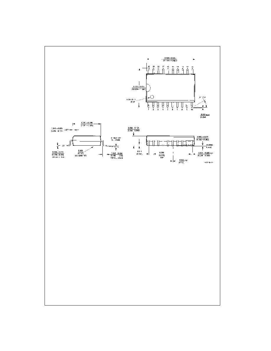
Physical Dimensions
inches (millimeters) unless otherwise noted
20-Lead Small Outline Integrated Circuit (SOIC), JEDEC MS-013, 0.300 Wide
Package Number M20B