 | –≠–ª–µ–∫—Ç—Ä–æ–Ω–Ω—ã–π –∫–æ–º–ø–æ–Ω–µ–Ω—Ç: 74FR245SJ | –°–∫–∞—á–∞—Ç—å:  PDF PDF  ZIP ZIP |
© 1999 Fairchild Semiconductor Corporation
DS010887
www.fairchildsemi.com
August 1990
Revised August 1999
7
4FR245
Oct
a
l Bidi
re
cti
onal T
r
a
nsceiv
e
r w
i
th 3-
ST
A
T
E O
u
t
put
s
74FR245
Octal Bidirectional Transceiver with 3-STATE Outputs
General Description
The 74FR245 contains eight non-inverting bidirectional
buffers with 3-STATE outputs and is intended for bus-ori-
ented applications. Current sinking capability is 64 mA on
both the A and B Ports. The Transmit/Receive (T/R) input
determines the direction of data flow through the bidirec-
tional transceiver. Transmit (active-HIGH) enables data
from A Ports to B Ports; Receive (active-LOW) enables
data from B Ports to A Ports. The Output Enable input,
when HIGH, disables both A and B Ports by placing them
in a High Z condition.
Features
s
Non-inverting buffers
s
Bidirectional data path
s
A and B output sink capability of 64 mA, source
capability of 15 mA
s
Guaranteed pin-to-pin skew
Ordering Code:
Devices also available in Tape and Reel. Specify by appending the suffix letter "X" to the ordering code.
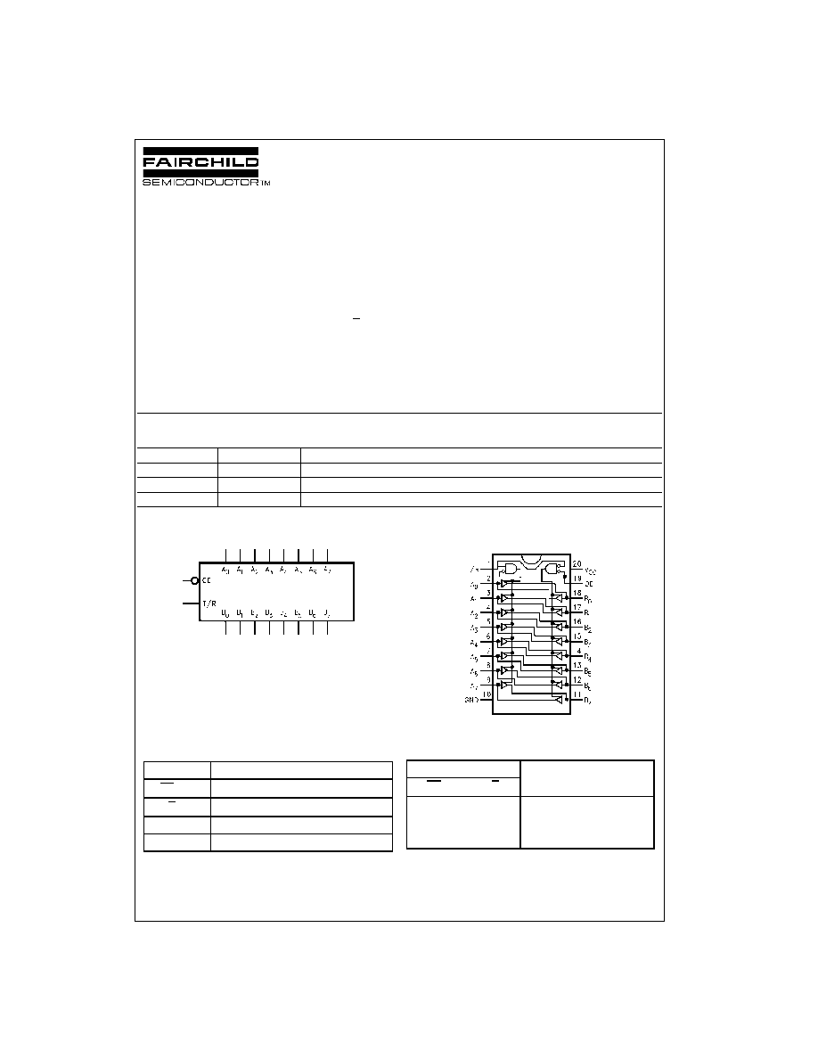
Logic Symbol
Pin Descriptions
Connection Diagram
Truth Table
H
=
HIGH Voltage Level
L
=
LOW Voltage Level
X
=
Immaterial
Order Number
Package Number
Package Description
74FR245SC
M20B
20-Lead Small Outline Integrated Circuit (SOIC), JEDEC MS-013, 0.300 Wide
74FR245SJ
M20D
20-Lead Small Outline Package (SOP), EIAJ TYPE II, 5.3mm Wide
74FR245PC
N20A
20-Lead Plastic Dual-In-Line Package (PDIP), JEDEC MS-001, 0.300 Wide
Pin Names
Description
OE
Output Enable Input (Active-LOW)
T/R
Transmit/Receive Input
A
0
≠A
7
Side A Inputs or 3-STATE Outputs
B
0
≠B
7
Side B Inputs or 3-STATE Outputs
Inputs
Output
OE
T/R
L
L
Bus B Data to Bus A
L
H
Bus A Data to Bus B
H
X
High Z State
www.fairchildsemi.com
2
74FR245
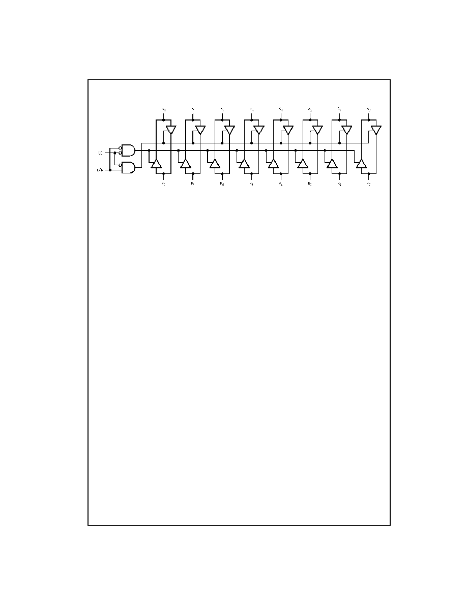
Logic Diagram
3
www.fairchildsemi.com
7
4FR245
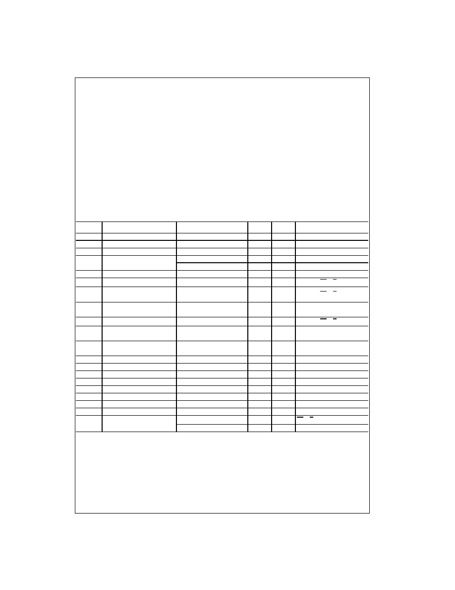
Absolute Maximum Ratings
(Note 1)
Recommended Operating
Conditions
Note 1: Absolute maximum ratings are values beyond which the device
may be damaged or have its useful life impaired. Functional operation
under these conditions is not implied.
Note 2: Either voltage limit or current limit is sufficient to protect inputs.
DC Electrical Characteristics
Storage Temperature
-
65
∞
C to
+
150
∞
C
Ambient Temperature under Bias
-
55
∞
C to
+
125
∞
C
Junction Temperature under Bias
-
55
∞
C to
+
150
∞
C
V
CC
Pin Potential to Ground Pin
-
0.5V to
+
7.0V
Input Voltage (Note 2)
-
0.5V to
+
7.0V
Input Current (Note 2)
-
30 mA to
+
5.0 mA
Voltage Applied to Output
in HIGH State (with V
CC
=
0V)
Standard Output
-
0.5V to V
CC
3-STATE Output
-
0.5V to
+
5.5V
Current Applied to Output
in LOW State (Max)
twice the rated I
OL
(mA)
ESD Last Passing Voltage (Min)
4000V
Free Air Ambient Temperature
0
∞
C to
+
70
∞
C
Supply Voltage
+
4.5V to
+
5.5V
Symbol
Parameter
Min
Typ
Max
Units
V
CC
Conditions
V
IH
Input HIGH Voltage
2.0
V
Recognized HIGH Signal
V
IL
Input LOW Voltage
0.8
V
Recognized LOW Signal
V
CD
Input Clamp Diode Voltage
-
1.2
V
Min
I
IN
=
-
18 mA
V
OH
Output HIGH Voltage
2.4
V
Min
I
OH
=
-
3 mA (A
n
, B
n
)
2.0
V
Min
I
OH
=
-
15 mA (A
n
, B
n
)
V
OL
Output LOW Voltage
0.55
V
Min
I
OL
=
64 mA (A
n
, B
n
)
I
IH
Input HIGH Current
5
µ
A
Max
V
IN
=
2.7V (OE, T/R)
I
BVI
Input HIGH Current
7
µ
A
Max
V
IN
=
7.0V (OE, T/R)
Breakdown Test
I
BVIT
Input HIGH Current
100
µ
A
Max
V
IN
=
5.5V (A
n
, B
n
)
Breakdown Test (I/O)
I
IL
Input LOW Current
-
250
µ
A
Max
V
IN
=
0.5V (OE, T/R)
V
ID
Input Leakage Test
4.75
V
0.0
I
ID
=
1.9
µ
A
All Other Pins Grounded
I
OD
Output Circuit
3.75
µ
A
0.0
V
IOD
=
150 mV
Leakage Current
All Other Pins Grounded
I
IH
+
I
OZH
Output Leakage Current
25
µ
A
Max
V
OUT
=
2.7V (A
n
, B
n
)
I
IL
+
I
OZL
Output Leakage Current
-
150
µ
A
Max
V
OUT
=
0.5V (A
n
, B
n
)
I
OS
Output Short-Circuit Current
-
100
-
225
mA
Max
V
OUT
=
0.0V (A
n
, B
n
)
I
CEX
Output HIGH Leakage Current
50
µ
A
Max
V
OUT
=
V
CC
(A
n
, B
n
)
I
ZZ
Bus Drainage Test
100
µ
A
0.0
V
OUT
=
5.25V (A
n
, B
n
)
I
CCH
Power Supply Current
55
75
mA
Max
All Outputs HIGH
I
CCL
Power Supply Current
75
110
mA
Max
All Outputs LOW
I
CCZ
Power Supply Current
55
75
mA
Max
Outputs 3-STATE
C
IN
Input Capacitance
8.0
pF
5.0
OE, T/R
17.0
pF
5.0
A
n
, B
n
www.fairchildsemi.com
4
74FR245
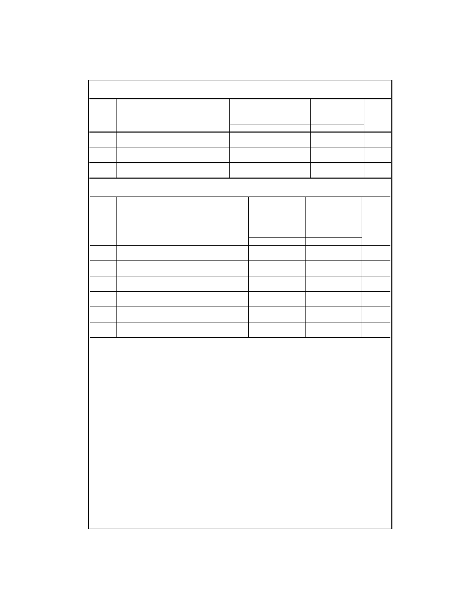
AC Electrical Characteristics
Extended AC Characteristics
Note 3: This specification is guaranteed but not tested. The limits apply to propagation delays for all paths described switching in phase, i.e., all LOW-to-
HIGH, HIGH-to-LOW, 3-STATE-to-HIGH, etc.
Note 4: These specifications guaranteed but not tested. The limits represent propagation delays with 250 pF load capacitors in place of the 50 pF load
capacitors in the standard AC load. This specification pertains to single output switching only.
Note 5: Skew is defined as the absolute value of the difference between the actual propagation delays for any two outputs of the same device. The specifi-
cation applies to any outputs switching HIGH-to-LOW (t
OSHL
), LOW-to-HIGH (t
OSLH
), or HIGH-to-LOW and/or LOW-to-HIGH (t
OST
). Specifications guaran-
teed with all outputs switching in phase.
Symbol
Parameter
T
A
=
+
25
∞
C
T
A
=
0
∞
C to
+
70
∞
C
Units
V
CC
=
+
5.0V
V
CC
=
+
5.0V
C
L
=
50 pF
C
L
=
50 pF
Min
Typ
Max
Min
Max
t
PLH
Propagation Delay
1.0
2.6
3.9
1.0
3.9
ns
t
PHL
A
n
to B
n
or B
n
to A
n
1.0
1.7
3.9
1.0
3.9
t
PZH
Output Enable Time
2.5
5.0
7.0
2.5
7.0
ns
t
PZL
2.5
4.3
7.0
2.5
7.0
t
PHZ
Output Disable Time
1.7
3.7
6.5
1.7
6.5
ns
t
PLZ
1.7
3.6
6.5
1.7
6.5
Symbol
Parameter
T
A
=
0
∞
C to
+
70
∞
C
T
A
=
0
∞
C to
+
70
∞
C
Units
V
CC
=
+
5.0V
V
CC
=
+
5.0V
C
L
=
50 pF
C
L
=
250 pF
Eight Outputs Switching
(Note 4)
(Note 3)
Min
Max
Min
Max
t
PLH
Propagation Delay
1.0
5.9
2.5
7.5
ns
t
PHL
A
n
to B
n
or B
n
to A
n
1.0
5.9
2.5
7.5
t
PZH
Output Enable Time
2.5
11.9
ns
t
PZL
2.5
11.9
t
PHZ
Output Disable Time
1.3
6.5
ns
t
PLZ
1.3
6.5
t
OSHL
Pin to Pin Skew
1.7
ns
(Note 5)
for HL Transitions
t
OSLH
Pin to Pin Skew
1.0
ns
(Note 5)
for LH Transitions
t
OST
Pin to Pin Skew
3.3
ns
(Note 5)
for HL/LH Transitions
5
www.fairchildsemi.com
7
4FR245
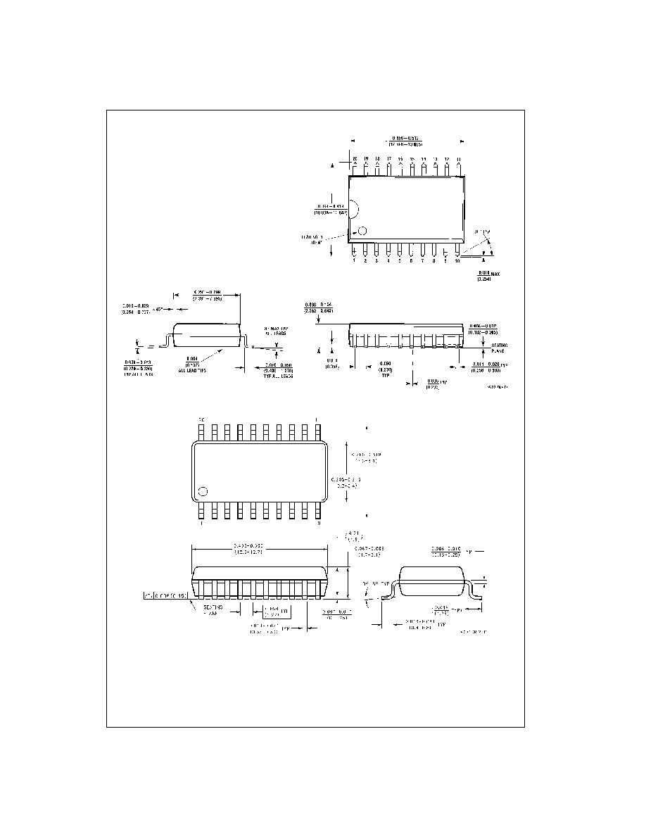
Physical Dimensions
inches (millimeters) unless otherwise noted
20-Lead Small Outline Integrated Circuit (SOIC), JEDEC MS-013, 0.300 Wide
Package Number M20B
20-Lead Small Outline Package (SOP), EIAJ TYPE II, 5.3mm Wide
Package Number M20D

www.fairchildsemi.com
6
74
FR245
Oct
a
l Bidi
rec
t
i
onal T
r
an
sceive
r
wi
th 3-
S
T
A
T
E O
u
t
puts
Physical Dimensions
inches (millimeters) unless otherwise noted (Continued)
20-Lead Plastic Dual-In-Line Package (PDIP), JEDEC MS-001, 0.300 Wide
Package Number N20A
Fairchild does not assume any responsibility for use of any circuitry described, no circuit patent licenses are implied and
Fairchild reserves the right at any time without notice to change said circuitry and specifications.
LIFE SUPPORT POLICY
FAIRCHILD'S PRODUCTS ARE NOT AUTHORIZED FOR USE AS CRITICAL COMPONENTS IN LIFE SUPPORT
DEVICES OR SYSTEMS WITHOUT THE EXPRESS WRITTEN APPROVAL OF THE PRESIDENT OF FAIRCHILD
SEMICONDUCTOR CORPORATION. As used herein:
1. Life support devices or systems are devices or systems
which, (a) are intended for surgical implant into the
body, or (b) support or sustain life, and (c) whose failure
to perform when properly used in accordance with
instructions for use provided in the labeling, can be rea-
sonably expected to result in a significant injury to the
user.
2. A critical component in any component of a life support
device or system whose failure to perform can be rea-
sonably expected to cause the failure of the life support
device or system, or to affect its safety or effectiveness.
www.fairchildsemi.com