 | –≠–ª–µ–∫—Ç—Ä–æ–Ω–Ω—ã–π –∫–æ–º–ø–æ–Ω–µ–Ω—Ç: 74LCX138M | –°–∫–∞—á–∞—Ç—å:  PDF PDF  ZIP ZIP |

© 2004 Fairchild Semiconductor Corporation
DS012417
www.fairchildsemi.com
March 1995
Revised February 2004
7
4
LCX138 Low
V
o
lt
age 1-
of
-8
Decoder/
Demult
ipl
exer
wit
h
5
V
T
o
le
rant
I
nputs
74LCX138
Low Voltage 1-of-8 Decoder/Demultiplexer
with 5V Tolerant Inputs
General Description
The LCX138 is a high-speed 1-of-8 decoder/demultiplexer.
This device is ideally suited for high-speed memory chip
select address decoding. The multiple input enables allow
parallel expansion to a 1-of-24 decoder using just three
LCX138 devices or a 1-of-32 decoder using four LCX138
devices and one inverter.
The 74LCX138 is fabricated with advanced CMOS technol-
ogy to achieve high speed operation while maintaining
CMOS low power dissipation.
Features
s
5V tolerant inputs
s
2.3V to 3.6V V
CC
specifications provided
s
6.0 ns t
PD
max (V
CC
=
3.3V), 10
µ
A I
CC
max
s
Power down high impedance inputs and outputs
s
±
24 mA output drive (V
CC
=
3.0V)
s
Implements patented noise/EMI reduction circuitry
s
Latch-up performance exceeds 500 mA
s
ESD performance:
Human body model
>
2000V
Machine model
>
200V
s
Leadless DQFN package
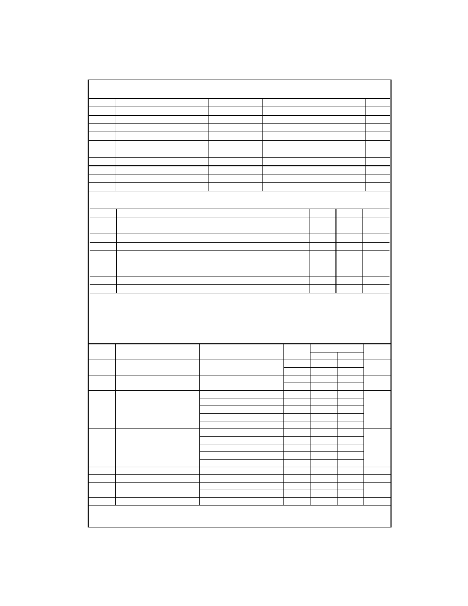
Ordering Code:
Note 1: Devices also available in Tape and Reel. Specify by appending suffix letter "X" to the ordering code.
Note 2: DQFN package available in Tape and Reel only.
Order Number
Package
Number
Package Description
74LCX138M
(Note 1)
M16A
16-Lead Small Outline Integrated Circuit (SOIC), JEDEC MS-012, 0.150" Narrow
74LCX138SJ
(Note 1)
M16D
16-Lead Small Outline Package (SOP), EIAJ TYPE II, 5.3mm Wide
74LCX138BQX
(Note 2)
MLP016E
16-Terminal Depopulated Quad Very-Thin Flat Pack No Leads (DQFN), JEDEC MO-241,
2.5 x 3.5mm
74LCX138MTC
(Note 1)
MTC16
16-Lead Thin Shrink Small Outline Package (TSSOP), JEDEC MO-153, 4.4mm Wide

www.fairchildsemi.com
2
74LCX138
Connection Diagrams
Pin Assignments for SOIC, SOP, and TSSOP
Pad Assignments for DQFN
(Top Through View)
Pin Descriptions
Functional Description
The LCX138 high-speed 1-of-8 decoder/demultiplexer
accepts three binary weighted inputs (A
0
, A
1
, A
2
) and,
when enabled, provides eight mutually exclusive active-
LOW outputs (O
0
≠O
7
). The LCX138 features three Enable
inputs, two active-LOW (E
1
, E
2
) and one active-HIGH (E
3
).
All outputs will be HIGH unless E
1
and E
2
are LOW and E
3
is HIGH. The LCX138 can be used as an 8-output demulti-
plexer by using one of the active LOW Enable inputs as the
data input and the other Enable inputs as strobes. The
Enable inputs which are not used must be permanently tied
to their appropriate active-HIGH or active-LOW state.
Truth Table
H
=
HIGH Voltage Level
L
=
LOW Voltage Level
X
=
Immaterial
Pin Names
Description
A
0
≠A
2
Address Inputs
E
1
≠E
2
Enable Inputs
E
3
Enable Input
O
0
≠O
7
Outputs
Inputs
Outputs
E
1
E
2
E
3
A
0
A
1
A
2
O
0
O
1
O
2
O
3
O
4
O
5
O
6
O
7
H
X
X
X
X
X
H
H
H
H
H
H
H
H
X
H
X
X
X
X
H
H
H
H
H
H
H
H
X
X
L
X
X
X
H
H
H
H
H
H
H
H
L
L
H
L
L
L
L
H
H
H
H
H
H
H
L
L
H
H
L
L
H
L
H
H
H
H
H
H
L
L
H
L
H
L
H
H
L
H
H
H
H
H
L
L
H
H
H
L
H
H
H
L
H
H
H
H
L
L
H
L
L
H
H
H
H
H
L
H
H
H
L
L
H
H
L
H
H
H
H
H
H
L
H
H
L
L
H
L
H
H
H
H
H
H
H
H
L
H
L
L
H
H
H
H
H
H
H
H
H
H
H
L

3
www.fairchildsemi.com
7
4
LCX138
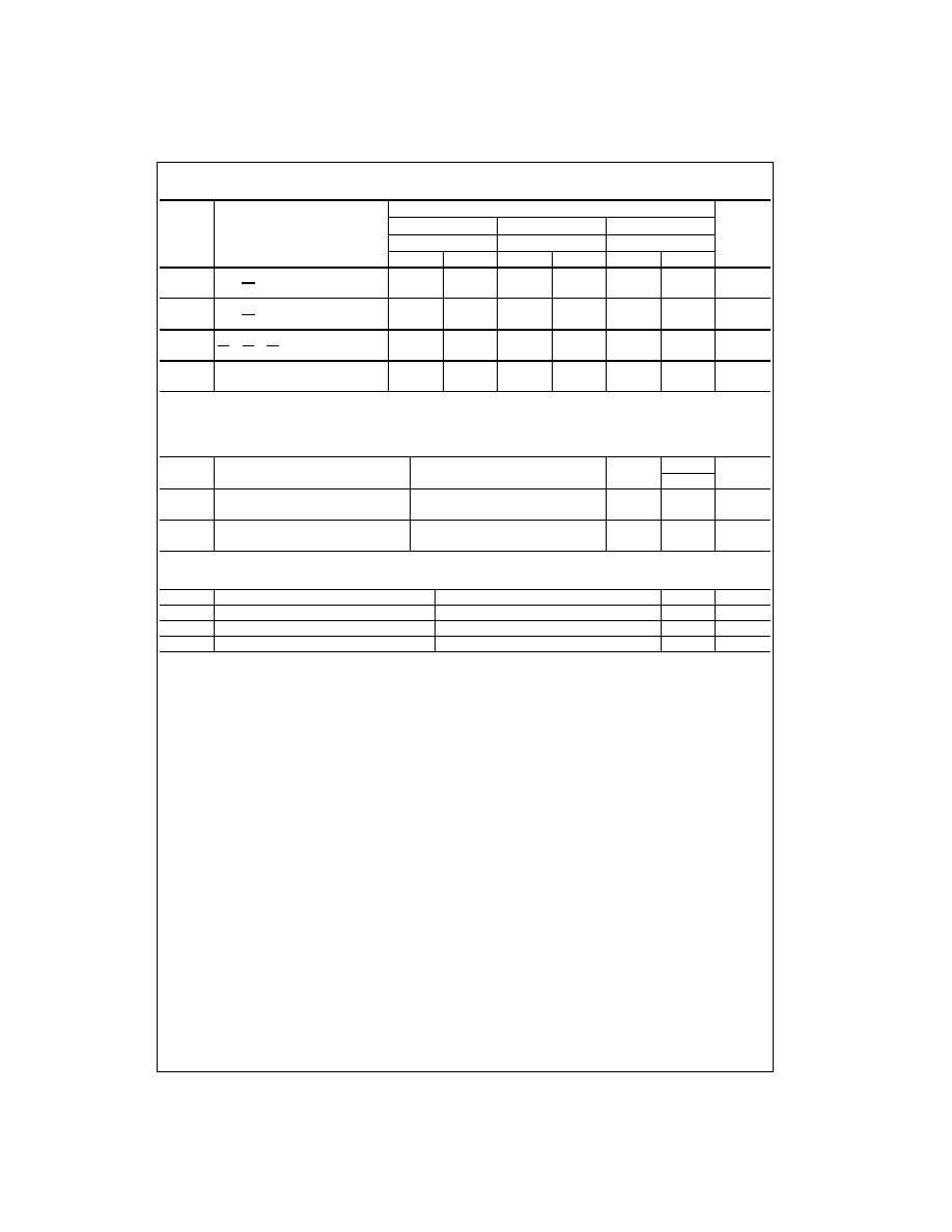
Logic Diagram
Please note that this diagram is provided only for the understanding of logic operations and should not be used to estimate propagation delays.
www.fairchildsemi.com
4
74LCX138
Absolute Maximum Ratings
(Note 3)
Recommended Operating Conditions
(Note 5)
Note 3: The Absolute Maximum Ratings are those values beyond which the safety of the device cannot be guaranteed. The device should not be operated
at these limits. The parametric values defined in the Electrical Characteristics tables are not guaranteed at the Absolute Maximum Ratings. The "Recom-
mended Operating Conditions" table will define the conditions for actual device operation.
Note 4: I
O
Absolute Maximum Rating must be observed.
Note 5: Unused inputs must be held HIGH or LOW. They may not float.
DC Electrical Characteristics
Symbol
Parameter
Value
Conditions
Units
V
CC
Supply Voltage
-
0.5 to
+
7.0
V
V
I
DC Input Voltage
-
0.5 to
+
7.0
V
V
O
DC Output Voltage
-
0.5 to V
CC
+
0.5
Output in HIGH or LOW State (Note 4)
V
I
IK
DC Input Diode Current
-
50
V
I
<
GND
mA
I
OK
DC Output Diode Current
-
50
V
O
<
GND
mA
+
50
V
O
>
V
CC
I
O
DC Output Source/Sink Current
±
50
mA
I
CC
DC Supply Current per Supply Pin
±
100
mA
I
GND
DC Ground Current per Ground Pin
±
100
mA
T
STG
Storage Temperature
-
65 to
+
150
∞
C
Symbol
Parameter
Min
Max
Units
V
CC
Supply Voltage
Operating
2.0
3.6
V
Data Retention
1.5
3.6
V
I
Input Voltage
0.0
5.5
V
V
O
Output Voltage
HIGH or LOW State
0.0
V
CC
V
I
OH
/I
OL
Output Current
V
CC
=
3.0V to 3.6V
±
24.0
mA
V
CC
=
2.7V to 3.0V
±
12.0
V
CC
=
2.3V to 2.7V
±
8.0
T
A
Free-Air Operating Temperature
-
40.0
85.0
∞
C
t/
V
Input Edge Rate, V
IN
=
0.8V to 2.0V, V
CC
=
3.0V
0.0
10.0
ns/V
Symbol
Parameter
Conditions
V
CC
T
A
=
-
40
∞
C to
+
85
∞
C
Units
(V)
Min
Max
V
IH
HIGH Level Input Voltage
2.3 to 2.7
1.7
V
2.7 to 3.6
2.0
V
IL
LOW Level Input Voltage
2.3 to 2.7
0.7
V
2.7 to 3.6
0.8
V
OH
HIGH Level Output Voltage
I
OH
=
-
100
µ
A
2.3 to 3.6
V
CC
-
0.2
V
I
OH
= -8 mA
2.3
1.8
I
OH
=
-
12 mA
2.7
2.2
I
OH
=
-
18 mA
3.0
2.4
I
OH
=
-
24 mA
3.0
2.2
V
OL
LOW Level Output Voltage
I
OL
=
100
µ
A
2.3 to 3.6
0.2
V
I
OL
= 8mA
2.3
0.6
I
OL
=
12 mA
2.7
0.4
I
OL
=
16 mA
3.0
0.4
I
OL
=
24 mA
3.0
0.55
I
I
Input Leakage Current
0
V
I
5.5V
2.3 to 3.6
±
5.0
µ
A
I
OFF
Power-Off Leakage Current
V
I
or V
O
=
5.5V
0.0
10.0
µ
A
I
CC
Quiescent Supply Current
V
I
=
V
CC
or GND
2.3 to 3.6
10.0
µ
A
3.6V
V
I
5.5V
2.3 to 3.6
±
10.0
I
CC
Increase in I
CC
per Input
V
IH
=
V
CC
-
0.6V
2.3 to 3.6
500
µ
A
5
www.fairchildsemi.com
7
4
LCX138
AC Electrical Characteristics
Note 6: Skew is defined as the absolute value of the difference between the actual propagation delay for any two separate outputs of the same device. The
specification applies to any outputs switching in the same direction, either HIGH-to-LOW (t
OSHL
) or LOW-to-HIGH (t
OSLH
).
Dynamic Switching Characteristics
Capacitance
Symbol
Parameter
T
A
=
-
40
∞
C to
+
85
∞
C, R
L
=
500
Units
V
CC
=
3.3V
±
0.3V
V
CC
=
2.7V
V
CC
=
2.5V
±
0.2V
C
L
=
50pF
C
L
=
50pF
C
L
=
30pF
Min
Max
Min
Max
Min
Max
t
PHL
Propagation Delay
1.5
6.0
1.5
7.0
1.5
7.2
ns
t
PLH
An to Qn
1.5
6.0
1.5
7.0
1.5
7.2
t
PHL
Propagation Delay
1.5
6.5
1.5
7.5
1.5
8.4
ns
t
PLH
E3 to Qn
1.5
6.5
1.5
7.5
1.5
8.4
t
PHL
Propagation Delay
1.5
6.0
1.5
7.0
1.5
7.2
ns
t
PLH
E1 or E2 to Qn
1.5
6.0
1.5
7.0
1.5
7.2
t
OSHL
Output to Output Skew (Note 6)
1.0
ns
t
OSLH
1.0
Symbol
Parameter
Conditions
V
CC
T
A
=
25
∞
C
Units
(V)
Typical
V
OLP
Quiet Output Dynamic Peak V
OL
C
L
=
50 pF, V
IH
=
3.3V, V
IL
=
0V
3.3
0.8
V
C
L
=
30 pF, V
IH
=
2.5V, V
IL
=
0V
2.5
0.6
V
OLV
Quiet Output Dynamic Valley V
OL
C
L
=
50 pF, V
IH
=
3.3V, V
IL
=
0V
3.3
-
0.8
V
C
L
=
30 pF, V
IH
=
2.5V, V
IL
=
0V
2.5
-
0.6
Symbol
Parameter
Conditions
Typical
Units
C
IN
Input Capacitance
V
CC
=
Open, V
I
=
0V or V
CC
7.0
pF
C
OUT
Output Capacitance
V
CC
=
3.3V, V
I
=
0V or V
CC
8.0
pF
C
PD
Power Dissipation Capacitance
V
CC
=
3.3V, V
I
=
0V or V
CC
, f
=
10 MHz
25.0
pF