Äîêóìåíòàöèÿ è îïèñàíèÿ www.docs.chipfind.ru
© 2001 Fairchild Semiconductor Corporation
DS500442
www.fairchildsemi.com
February 2001
Revised August 2001
7
4
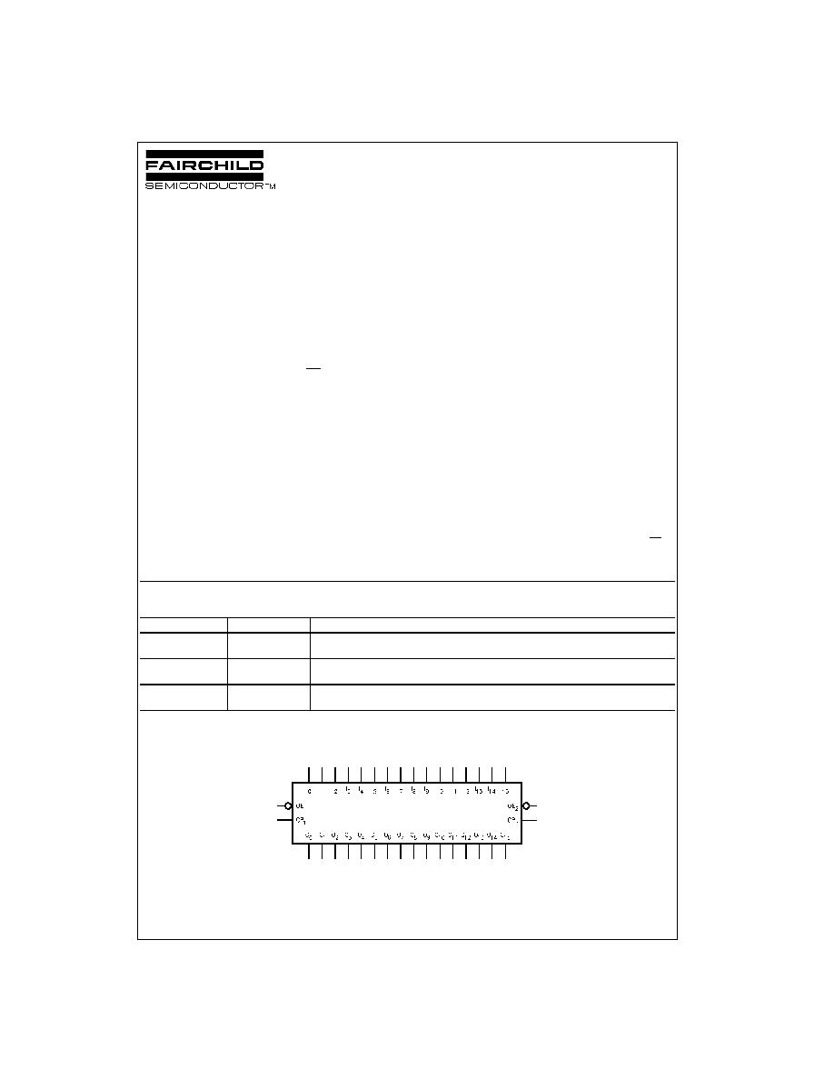
LCX162374
Low
V
o
lt
age 16
-Bit
D-
T
y
pe Fl
i
p
-Fl
op wi
th
5V T
o
le
rant
I
nputs
and Out
puts
and
26
Seri
es
Res
i
st
ors
74LCX162374
Low Voltage 16-Bit D-Type Flip-Flop
with 5V Tolerant Inputs and Outputs
and 26
Series Resistors
General Description
The LCX162374 contains sixteen non-inverting D-type
flip-flops with 3-STATE outputs and is intended for bus ori-
ented applications. The device is byte controlled. A buff-
ered clock (CP) and Output Enable (OE) are common to
each byte and can be shorted together for full 16-bit opera-
tion.
The LCX162374 is designed for low voltage (2.5V or 3.3V)
V
CC
applications with capability of interfacing to a 5V signal
environment. The 26
series resistor in the output helps
reduce output overshoot and undershoot.
The LCX162374 is fabricated with an advanced CMOS
technology to achieve high speed operation while maintain-
ing CMOS low power dissipation.
Features
I
5V tolerant inputs and outputs
I
2.3V3.6V V
CC
specifications provided
I
Equivalent 26
series resistor on outputs
I
7.0 ns t
PD
max (V
CC
=
3.3V), 20
µ
A I
CC
max
I
Power down high impedance inputs and outputs
I
Supports live insertion/withdrawal (Note 1)
I
±
12 mA output drive (V
CC
=
3.0V)
I
Implements patented noise/EMI reduction circuitry
I
Latch-up performance exceeds 500 mA
I
ESD performance:
Human body model
>
2000V
Machine model
>
200V
I
Also packaged in plastic Fine-Pitch Ball Grid Array
(FBGA) (Preliminary)
Note 1: To ensure the high-impedance state during power up or down, OE
should be tied to V
CC
through a pull-up resistor: the minimum value or the
resistor is determined by the current-sourcing capability of the driver.
Ordering Code:
Note 2: BGA package available in Tape and Reel only.
Note 3: Devices also available in Tape and Reel. Specify by appending the suffix letter "X" to the ordering code.
Logic Symbol
Order Number
Package Number
Package Description
74LCX162374GX
(Note 2)
BGA54A
(Preliminary)
54-Ball Fine-Pitch Ball Grid Array (FBGA), JEDEC MO-205, 5.5mm Wide
[TAPE and REEL]
74LCX162374MEA
(Note 3)
MS48A
48-Lead Small Shrink Outline Package (SSOP), JEDEC MO-118, 0.300" Wide
74LCX162374MTD
(Note 3)
MTD48
48-Lead Thin Shrink Small Outline Package (TSSOP), JEDEC MO-153, 6.1mm Wide
www.fairchildsemi.com
2
74LCX162374
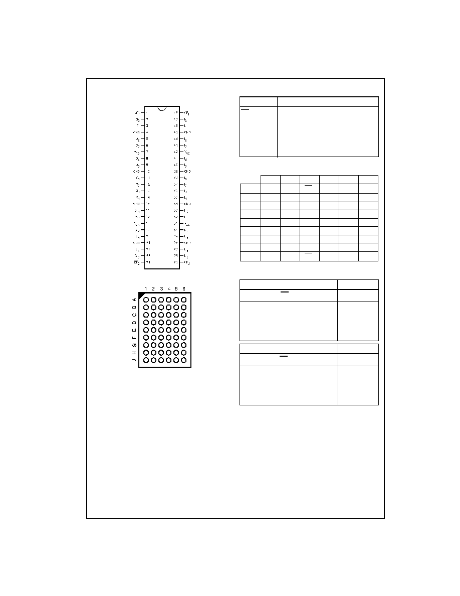
Connection Diagrams
Pin Assignment for SSOP and TSSOP
Pin Assignment for FBGA
(Top Thru View)
Pin Descriptions
FBGA Pin Assignments
Truth Tables
H
=
HIGH Voltage Level
L
=
LOW Voltage Level
X
=
Immaterial
Z
=
High Impedance
O
0
=
Previous O
0
before HIGH-to-LOW of CP
Pin Names
Description
OE
n
Output Enable Input (Active LOW)
CP
n
Clock Pulse Input
I
0
I
15
Inputs
O
0
O
15
Outputs
NC
No Connect
1
2
3
4
5
6
A
O
0
NC
OE
1
CP
1
NC
I
0
B
O
2
O
1
NC
NC
I
1
I
2
C
O
4
O
3
V
CC
V
CC
I
3
I
4
D
O
6
O
5
GND
GND
I
5
I
6
E
O
8
O
7
GND
GND
I
7
I
8
F
O
10
O
9
GND
GND
I
9
I
10
G
O
12
O
11
V
CC
V
CC
I
11
I
12
H
O
14
O
13
NC
NC
I
13
I
14
J
O
15
NC
OE
2
CP
2
NC
I
15
Inputs
Outputs
CP
1
OE
1
I
0
I
7
O
0
O
7
L
H
H
L
L
L
L
L
X
O
0
X
H
X
Z
Inputs
Outputs
CP
2
OE
2
I
8
I
15
O
8
O
15
L
H
H
L
L
L
L
L
X
O
0
X
H
X
Z
3
www.fairchildsemi.com
7
4
LCX162374
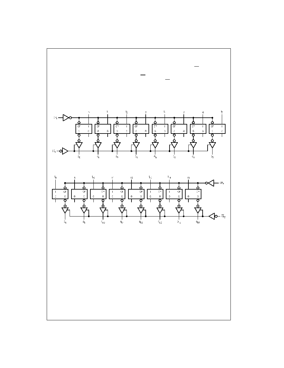
Functional Description
The LCX162374 consists of sixteen edge-triggered
flip-flops with individual D-type inputs and 3-STATE true
outputs. The device is byte controlled with each byte func-
tioning identically, but independent of the other. The control
pins can be shorted together to obtain full 16-bit operation.
Each byte has a buffered clock and buffered Output Enable
common to all flip-flops within that byte. The description
which follows applies to each byte. Each flip-flop will store
the state of their individual D inputs that meet the setup and
hold time requirements on the LOW-to-HIGH Clock (CP
n
)
transition. With the Output Enable (OE
n
) LOW, the con-
tents of the flip-flops are available at the outputs. When
OE
n
is HIGH, the outputs go to the high impedance state.
Operation of the OE
n
input does not affect the state of the
flip-flops.
Logic Diagrams
Byte 1 (0:7)
Byte 2 (8:15)
Please note that this diagram is provided only for the understanding of logic operations and should not be used to estimate propagation delays.
www.fairchildsemi.com
4
74LCX162374
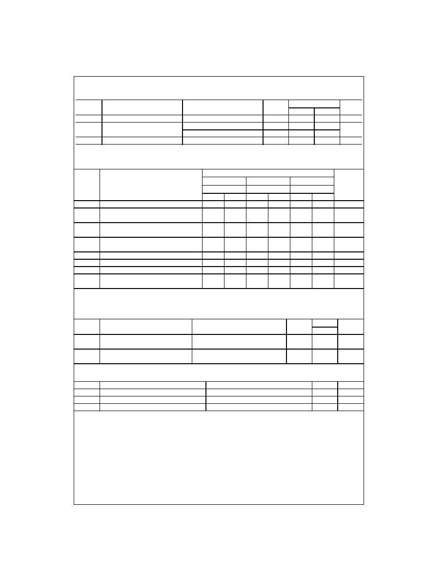
Absolute Maximum Ratings
(Note 4)
Recommended Operating Conditions
(Note 6)
Note 4: The Absolute Maximum Ratings are those values beyond which the safety of the device cannot be guaranteed. The device should not be operated
at these limits. The parametric values defined in the Electrical Characteristics tables are not guaranteed at the Absolute Maximum Ratings. The "Recom-
mended Operating Conditions" table will define the conditions for actual device operation.
Note 5: I
O
Absolute Maximum Rating must be observed.
Note 6: Floating or unused control inputs must be HIGH or LOW.
DC Electrical Characteristics
Symbol
Parameter
Value
Conditions
Units
V
CC
Supply Voltage
-
0.5 to
+
7.0
V
V
I
DC Input Voltage
-
0.5 to
+
7.0
V
V
O
DC Output Voltage
-
0.5 to
+
7.0
3-STATE
V
-
0.5 to V
CC
+
0.5
Output in HIGH or LOW State (Note 5)
I
IK
DC Input Diode Current
-
50
V
I
<
GND
mA
I
OK
DC Output Diode Current
-
50
V
O
<
GND
mA
+
50
V
O
>
V
CC
I
O
DC Output Source/Sink Current
±
50
mA
I
CC
DC Supply Current per Supply Pin
±
100
mA
I
GND
DC Ground Current per Ground Pin
±
100
mA
T
STG
Storage Temperature
-
65 to
+
150
°
C
Symbol
Parameter
Min
Max
Units
V
CC
Supply Voltage
Operating
2.0
3.6
V
Data Retention
1.5
3.6
V
I
Input Voltage
0
5.5
V
V
O
Output Voltage
HIGH or LOW State
0
V
CC
V
3-STATE
0
5.5
I
OH
/I
OL
Output Current
V
CC
=
3.0V
-
3.6V
±
12
mA
V
CC
=
2.7V
-
3.0V
±
8
V
CC
=
2.3V
-
2.7V
±
4
T
A
Free-Air Operating Temperature
-
40
85
°
C
t/
V
Input Edge Rate, V
IN
=
0.8V2.0V, V
CC
=
3.0V
0
10
ns/V
Symbol
Parameter
Conditions
V
CC
T
A
=
-
40
°
C to
+
85
°
C
Units
(V)
Min
Max
V
IH
HIGH Level Input Voltage
2.3
-
2.7
1.7
V
2.7
-
3.6
2.0
V
IL
LOW Level Input Voltage
2.3
-
2.7
0.7
V
2.7
-
3.6
0.8
V
OH
HIGH Level Output Voltage
I
OH
=
-
100
µ
A
2.3
-
3.6
V
CC
-
0.2
V
I
OH
=
-
4 mA
2.3
1.8
I
OH
=
-
4 mA
2.7
2.2
I
OH
=
-
6 mA
3.0
2.4
I
OH
=
-
8 mA
2.7
2.0
I
OH
=
-
12 mA
3.0
2.0
V
OL
LOW Level Output Voltage
I
OL
=
100
µ
A
2.3
-
3.6
0.2
V
I
OL
=
4 mA
2.3
0.6
I
OL
=
4 mA
2.7
0.4
I
OL
=
6 mA
3.0
0.55
I
OL
=
8 mA
2.7
0.6
I
OL
=
12 mA
3.0
0.8
I
I
Input Leakage Current
0
V
I
5.5V
2.3
-
3.6
±
5.0
µ
A
I
OZ
3-STATE Output Leakage
0
V
O
5.5V
2.3
-
3.6
±
5.0
µ
A
V
I
=
V
IH
or V
IL
5
www.fairchildsemi.com
7
4
LCX162374
DC Electrical Characteristics
(Continued)
Note 7: Outputs disabled or 3-STATE only.
AC Electrical Characteristics
Note 8: Skew is defined as the absolute value of the differences between the actual propagation delay for any two separate outputs of the same device. The
specification applies to any outputs switching in the same direction, either HIGH-to-LOW (t
OSHL
) or LOW-to-HIGH (t
OSLH
). Parameter guaranteed by design.
Dynamic Switching Characteristics
Capacitance
Symbol
Parameter
Conditions
V
CC
T
A
=
-
40
°
C to
+
85
°
C
Units
(V)
Min
Max
I
OFF
Power-Off Leakage Current
V
I
or V
O
=
5.5V
0
10
µ
A
I
CC
Quiescent Supply Current
V
I
=
V
CC
or GND
2.3
-
3.6
20
µ
A
3.6V
V
I
, V
O
5.5V (Note 7)
2.3
-
3.6
±
20
I
CC
Increase in I
CC
per Input
V
IH
=
V
CC
-
0.6V
2.3
-
3.6
500
µ
A
Symbol
Parameter
T
A
=
-
40
°
to
+
85
°
C, R
L
=
500
Units
V
CC
=
3.3V
±
0.3V
V
CC
=
2.7V
V
CC
=
2.5V
±
0.2V
C
L
=
50 pF
C
L
=
50 pF
C
L
=
30 pF
Min
Max
Min
Max
Min
Max
f
MAX
Maximum Clock Frequency
170
MHz
t
PHL
Propagation Delay
1.5
7.0
1.5
7.3
1.5
8.4
ns
t
PLH
CP to O
n
1.5
7.0
1.5
7.3
1.5
8.4
t
PZL
Output Enable time
1.5
6.9
1.5
7.1
1.5
9.0
ns
t
PZH
1.5
6.9
1.5
7.1
1.5
9.0
t
PLZ
Output Disable Time
1.5
6.0
1.5
6.2
1.5
7.2
ns
t
PHZ
1.5
6.0
1.5
6.2
1.5
7.2
t
S
Setup Time
2.5
2.5
3.0
ns
t
H
Hold Time
1.5
1.5
2.0
ns
t
W
Pulse Width
3.0
3.0
3.5
ns
t
OSHL
Output to Output Skew (Note 8)
1.0
ns
t
OSLH
1.0
Symbol
Parameter
Conditions
V
CC
T
A
=
25
°
C
Units
(V)
Typical
V
OLP
Quiet Output Dynamic Peak V
OL
C
L
=
50 pF, V
IH
=
3.3V, V
IL
=
0V
3.3
0.35
V
C
L
=
30 pF, V
IH
=
2.5V, V
IL
=
0V
2.5
0.25
V
OLV
Quiet Output Dynamic Valley V
OL
C
L
=
50 pF, V
IH
=
3.3V, V
IL
=
0V
3.3
-
0.35
V
C
L
=
30 pF, V
IH
=
2.5V, V
IL
=
0V
2.5
-
0.25
Symbol
Parameter
Conditions
Typical
Units
C
IN
Input Capacitance
V
CC
=
Open, V
I
=
0V or V
CC
7
pF
C
OUT
Output Capacitance
V
CC
=
3.3V, V
I
=
0V or V
CC
8
pF
C
PD
Power Dissipation Capacitance
V
CC
=
3.3V, V
I
=
0V or V
CC
, f
=
10 MHz
20
pF