
October 1995
Revised April 1999
7
4LCX16501 18-Bi
t Univer
sal
Bus T
r
ansc
eiver
s
wi
th 5V
T
o
l
e
rant
Input
s
an
d
Outp
uts
© 1999 Fairchild Semiconductor Corporation
DS012550.prf
www.fairchildsemi.com
74LCX16501
18-Bit Universal Bus Transceivers with 5V Tolerant
Inputs and Outputs
General Description
The LCX16501 is an 18-bit universal bus transceiver com-
bining D-type latches and D-type flip-flops to allow data
flow in transparent, latched, and clocked modes.
Data flow in each direction is controlled by output-enable
(OEAB and OEBA), latch-enable (LEAB and LEBA), and
clock (CLKAB and CLKBA) inputs.
The LCX16501 is designed for low voltage (2.5V or 3.3V)
V
CC
applications with capability of interfacing to a 5V signal
environment.
The LCX16501 is fabricated with an advanced CMOS tech-
nology to achieve high speed operation while maintaining
CMOS low power.
Features
s
5V tolerant inputs and outputs
s
2.3V≠3.6V V
CC
specifications provided
s
6.0 ns t
PD
max (V
CC
=
3.3V), 20
µ
A I
CC
max
s
Power down high impedance inputs and outputs
s
Supports live insertion/withdrawal (Note 1)
s
±
24 mA Output Drive (V
CC
=
3.0V)
s
Implements patented noise/EMI reduction circuitry
s
Latch-up performance exceeds 500 mA
s
ESD performance:
Human body model
>
2000V
Machine model
<
200V
Note 1: To ensure the high-impedance state during power up or down, OE
should be tied to V
CC
and OE tied to GND through a resistor: the minimum
value or the resistor is determined by the current-sourcing capability of the
driver.
Ordering Code:
Devices also available on Tape and Reel. Specify by appending the suffix letter "X" to the ordering code.
Order Number
Package Number
Package Description
74LCX16501MEA
MS56A
56-Lead Shrink Small Outline Package (SSOP), JEDEC MO-118, 0.300" Wide
74LCX16501MTD
MTD56
56-Lead Thin Shrink Small Outline Package (TSSOP), JEDEC MO-153, 6.1mm Wide
www.fairchildsemi.com
2
74LCX16501
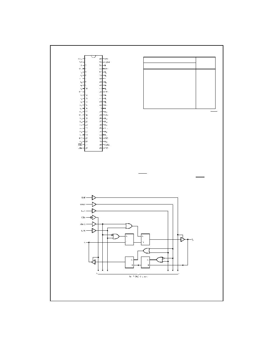
Connection Diagram
Truth Table
(Note 2)
Note 2: A-to-B data flow is shown: B-to-A flow is similar but uses OEBA,
LEBA, and CLKBA.
Note 3: Output level before the indicated steady-state input conditions
were established, provided that CLKAB was HIGH before LEAB went LOW.
Note 4: Output level before the indicated steady-state input conditions
were established.
Functional Description
For A-to-B data flow, the LCX16501 operates in the trans-
parent mode when LEAB is HIGH. When LEAB is LOW,
the A data is latched if CLKAB is held at a high or low logic
level. If LEAB is LOW, the A bus data is stored in the latch/
flip-flop on the LOW-to-HIGH transition of CLKAB. When
OEAB is HIGH, the outputs are active. When OEAB is
LOW, the outputs are in the high impedance state.
Data flow for B to A is similar to that of A to B but uses
OEBA, LEBA, and CLKBA. The output enables are com-
plementary (OEAB is active HIGH and OEBA is active
LOW).
Logic Diagram
Inputs
Output
OEAB
LEAB
CLKAB
A
n
B
n
L
X
X
X
Z
H
H
X
L
L
H
H
X
H
H
H
L
L
L
H
L
H
H
H
L
H
X
B
0
(Note 3)
H
L
L
X
B
0
(Note 4)
3
www.fairchildsemi.com
7
4LCX16501
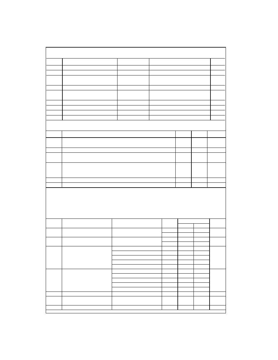
Absolute Maximum Ratings
(Note 5)
Recommended Operating Conditions
(Note 7)
Note 5: The Absolute Maximum Ratings are those values beyond which the safety of the device cannot be guaranteed. The device should not be operated
at these limits. The parametric values defined in the Electrical Characteristics tables are not guaranteed at the Absolute Maximum Ratings. The "Recom-
mended Operating Conditions" table will define the conditions for actual device operation.
Note 6: I
O
Absolute Maximum Rating must be observed.
Note 7: Unused (inputs or I/Os) must be held HIGH or LOW. They may not float.
DC Electrical Characteristics
Symbol
Parameter
Value
Conditions
Units
V
CC
Supply Voltage
-
0.5 to
+
7.0
V
V
I
DC Input Voltage
-
0.5 to
+
7.0
V
V
O
DC Output Voltage
-
0.5 to
+
7.0
Output in 3-STATE
V
-
0.5 to V
CC
+
0.5
Output in HIGH or LOW State (Note 6)
I
IK
DC Input Diode Current
-
50
V
I
<
GND
mA
I
OK
DC Output Diode Current
-
50
V
O
<
GND
mA
+
50
V
O
>
V
CC
I
O
DC Output Source/Sink Current
±
50
mA
I
CC
DC Supply Current per Supply Pin
±
100
mA
I
GND
DC Ground Current per Ground Pin
±
100
mA
T
STG
Storage Temperature
-
65 to
+
150
∞
C
Symbol
Parameter
Min
Max
Units
V
CC
Supply Voltage
Operating
2.0
3.6
V
Data Retention
1.5
3.6
V
I
Input Voltage
0
5.5
V
V
O
Output Voltage
HIGH or LOW State
0
V
CC
V
3-STATE
0
5.5
I
OH
/I
OL
Output Current
V
CC
=
3.0V
-
3.6V
±
24
mA
V
CC
=
2.7V
-
3.0V
±
12
V
CC
=
2.3V
-
2.7V
±
8
T
A
Free-Air Operating Temperature
-
40
85
∞
C
t/
V
Input Edge Rate, V
IN
=
0.8V≠2.0V, V
CC
=
3.0V
0
10
ns/V
Symbol
Parameter
Conditions
V
CC
T
A
=
-
40
∞
C to
+
85
∞
C
Units
(V)
Min
Max
V
IH
HIGH Level Input Voltage
2.3
-
2.7
1.7
V
2.7
-
3.6
2.0
V
IL
LOW Level Input Voltage
2.3
-
2.7
0.7
V
2.7
-
3.6
0.8
V
OH
HIGH Level Output Voltage
I
OH
=
-
100
µ
A
2.3
-
3.6
V
CC
-
0.2
V
I
OH
=
-
8 mA
2.3
1.8
I
OH
=
-
12 mA
2.7
2.2
I
OH
=
-
18 mA
3.0
2.4
I
OH
=
-
24 mA
3.0
2.2
V
OL
LOW Level Output Voltage
I
OL
=
100
µ
A
2.3
-
3.6
0.2
V
I
OL
=
8 mA
2.3
0.6
I
OL
=
12 mA
2.7
0.4
I
OL
=
16 mA
3.0
0.4
I
OL
=
24 mA
3.0
0.55
I
I
Input Leakage Current
0
V
I
5.5V
2.3
-
3.6
±
5.0
µ
A
I
OZ
3-STATE I/O Leakage
0
V
O
5.5V
2.3
-
3.6
±
5.0
µ
A
V
I
=
V
IH
or V
IL
I
OFF
Power-Off Leakage Current
V
I
or V
O
=
5.5V
0
10
µ
A

www.fairchildsemi.com
4
74LCX16501
DC Electrical Characteristics
(Continued)
Note 8: Outputs disabled or 3-STATE only.
AC Electrical Characteristics
Note 9: Skew is defined as the absolute value of the difference between the actual propagation delay for any two separate outputs of the same device. The
specification applies to any outputs switching in the same direction, either HIGH
-
to
-
LOW (t
OSHL
), or LOW
-
to
-
HIGH (t
OSLH
).
Dynamic Switching Characteristics
Capacitance
Symbol
Parameter
Conditions
V
CC
T
A
=
-
40
∞
C to
+
85
∞
C
Units
(V)
Min
Max
I
CC
Quiescent Supply Current
V
I
=
V
CC
or GND
2.3
-
3.6
20
µ
A
3.6V
V
I
, V
O
5.5V (Note 8)
2.3
-
3.6
±
20
I
CC
Increase in I
CC
per Input
V
IH
=
V
CC
-
0.6V
2.3
-
3.6
500
µ
A
Symbol
Parameter
T
A
=
-
40
∞
C to
+
85
∞
C, R
L
=
500
Units
V
CC
=
3.3V
±
0.3V
V
CC
=
2.7V
V
CC
=
2.5V
±
0.2V
C
L
=
50 pF
C
L
=
50 pF
C
L
=
30 pF
Min
Max
Min
Max
Min
Max
f
MAX
Maximum Clock Frequency
170
MHz
t
PHL
Propagation Delay
1.5
6.0
1.5
7.0
1.5
7.2
ns
t
PLH
Bus to Bus
1.5
6.0
1.5
7.0
1.5
7.2
t
PHL
Propagation Delay
1.5
6.7
1.5
8.0
1.5
8.4
ns
t
PLH
Clock to Bus
1.5
6.7
1.5
8.0
1.5
8.4
t
PHL
Propagation Delay
1.5
7.0
1.5
8.0
1.5
8.4
ns
t
PLH
LE to Bus
1.5
7.0
1.5
8.0
1.5
8.4
t
PZL
Output Enable Time
1.5
7.2
1.5
8.2
1.5
9.4
ns
t
PZH
1.5
7.2
1.5
8.2
1.5
9.4
t
PLZ
Output Disable Time
1.5
7.0
1.5
8.0
1.5
8.4
ns
t
PHZ
1.5
7.0
1.5
8.0
1.5
8.4
t
S
Setup Time
2.5
2.5
3.0
ns
t
H
Hold Time
1.5
1.5
2.0
ns
t
W
Pulse Width
3.0
3.0
3.5
ns
t
OSHL
Output to Output Skew
1.0
ns
t
OSLH
(Note 9)
1.0
Symbol
Parameter
Conditions
V
CC
(V)
T
A
=
25
∞
C
Units
Typical
V
OLP
Quiet Output Dynamic Peak V
OL
C
L
=
50 pF, V
IH
=
3.3V, V
IL
=
0V
3.3
0.8
V
C
L
=
30 pF, V
IH
=
2.5V, V
IL
=
0V
2.5
0.6
V
OLV
Quiet Output Dynamic Valley V
OL
C
L
=
50 pF, V
IH
=
3.3V, V
IL
=
0V
3.3
-
0.8
V
C
L
=
30 pF, V
IH
=
2.5V, V
IL
=
0V
2.5
-
0.6
Symbol
Parameter
Conditions
Typical
Units
C
IN
Input Capacitance
V
CC
=
Open, V
I
=
0V or V
CC
7
pF
C
I/O
Input/Output Capacitance
V
CC
=
3.3V, V
I
=
0V or V
CC
8
pF
C
PD
Power Dissipation Capacitance
V
CC
=
3.3V, V
I
=
0V or V
CC
, f
=
10 MHz
20
pF

5
www.fairchildsemi.com
7
4LCX16501
AC LOADING and WAVEFORMS
Generic for LCX Family
FIGURE 1. AC Test Circuit (C
L
includes probe and jig capacitance)
Waveform for Inverting and Non-Inverting Functions
Propagation Delay. Pulse Width and t
rec
Waveforms
3-STATE Output Low Enable and
Disable Times for Logic
3-STATE Output High Enable and
Disable Times for Logic
Setup Time, Hold Time and Recovery Time for Logic
t
rise
and t
fall
FIGURE 2. Waveforms
(Input Characteristics; f =1MHz, t
R
= t
F
= 3ns)
Test
Switch
t
PLH
, t
PHL
Open
t
PZL
, t
PLZ
6V at V
CC
=
3.3
±
0.3V
V
CC
x 2 at V
CC
=
2.5
±
0.2V
t
PZH
,t
PHZ
GND
Symbol
V
CC
3.3V
±
0.3V
2.7V
2.5V
±
0.2V
V
mi
1.5V
1.5V
V
CC
/2
V
mo
1.5V
1.5V
V
CC
/2
V
x
V
OL
+
0.3V
V
OL
+
0.3V
V
OL
+
0.15V
V
y
V
OH
-
0.3V
V
OH
-
0.3V
V
OH
-
0.15V