Preliminary
© 2001 Fairchild Semiconductor Corporation
DS500635
www.fairchildsemi.com
August 2001
Revised August 2001
7
4
LCX32646 Low
V
o
lt
age 32-Bi
t T
r
ans
ceiver
/Regi
s
t
e
r w
i
th 5V T
o
ler
a
nt Input
s and
Out
puts (
P
r
e
li
minar
y
)
74LCX32646
Low Voltage 32-Bit Transceiver/Register
with 5V Tolerant Inputs and Outputs (Preliminary)
General Description
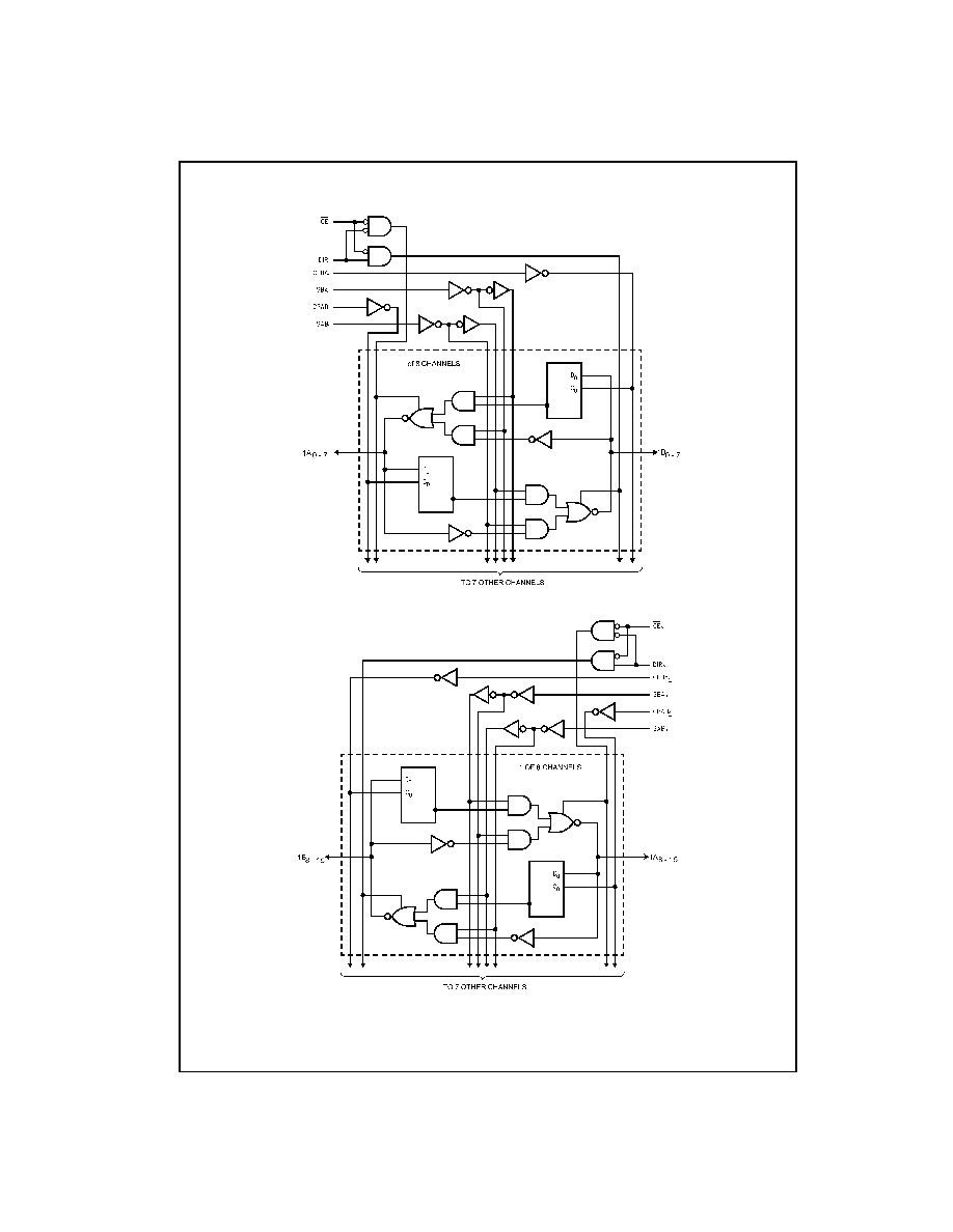
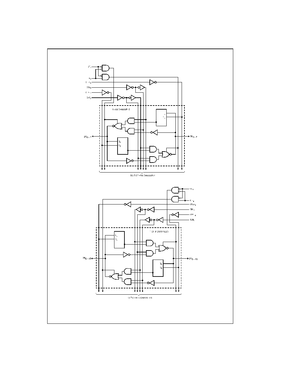
The LCX32646 contains thirty-two non-inverting bidirec-
tional registered bus transceivers with 3-STATE outputs,
providing multiplexed transmission of data directly from the
input bus or from the internal storage registers. Each byte
has separate control inputs which can be shorted together
for full 32-bit operation.The DIR
n
inputs determine the
direction of data flow through the device. The CPAB
n
and
CPBA
n
inputs load data into the registers on the LOW-to-
HIGH transition (see Functional Description).
The LCX32646 is designed for low voltage (2.5V or 3.3V)
V
CC
applications with capability of interfacing to a 5V signal
environment.
The LCX32646 is fabricated with an advanced CMOS tech-
nology to achieve high speed operation while maintaining
CMOS low power dissipation.
Features
s
5V tolerant inputs and outputs
s
2.3V3.6V V
CC
specifications provided
s
5.2 ns t
PD
max (V
CC
=
3.3V), 20
µ
A I
CC
max
s
Power down high impedance inputs and outputs
s
Supports live insertion/withdrawal (Note 1)
s
±
24 mA Output Drive (V
CC
=
3.0V)
s
Implements patented noise/EMI reduction circuitry
s
Latch-up performance exceeds 500 mA
s
ESD performance:
Human Body Model
>
2000V
Machine Model
>
200V
s
Packaged in plastic Fine-Pitch Ball Grid Array (FBGA)
(Preliminary)
Note 1: To ensure the high-impedance state during power up or down, OE
should be tied to V
CC
through a pull-up resistor: the minimum value or the
resistor is determined by the current-sourcing capability of the driver.
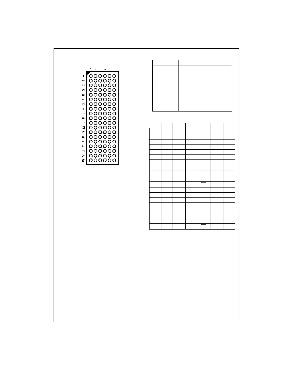
Ordering Code:
Note 2: BGA package available in Tape and Reel only.
Order Number
Package Number
Package Description
74LCX32646GX
(Note 2)
BGA114A
(Preliminary)
114-Ball Fine-Pitch Ball Grid Array (FBGA), JEDEC MO-205, 5.5mm Wide
[TAPE and REEL]
Preliminary
3
www.fairchildsemi.com
7
4
LCX32646
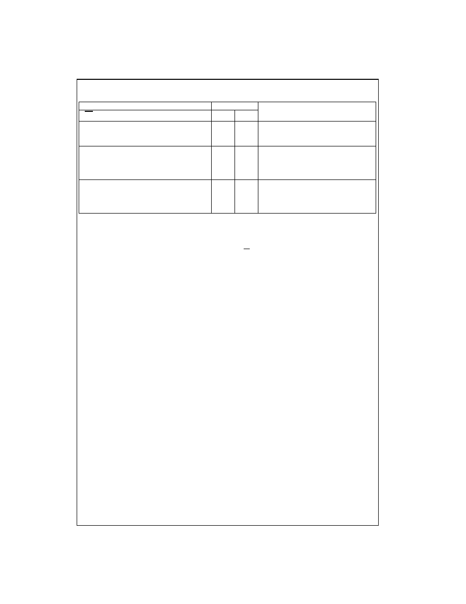
Truth Table
(Note 3)
H
=
HIGH Voltage Level
L
=
LOW Voltage Level
X
=
Immaterial
=
LOW-to-HIGH Transition
Note 3: Data I/O paths (1A and 1B: 0 - 7) is shown. This also applies to data I/O (1A and 1B: 8 - 15) and #2 control pins, to data (2A and 2B: 0 - 7) and #3
control pins, to data (2A and 2B: 8 - 15) and #4 control pins.
Note 4: The data output functions may be enabled or disabled by various signals at the OE and DIR inputs. Data input functions are always enabled;
i.e., data at the bus pins will be stored on every LOW-to-HIGH transition of the appropriate clock inputs.
Inputs
Data I/O (Note 4)
Output Operation Mode
OE
1
DIR
1
CPAB
1
CPBA
1
SAB
1
SBA
1
1A
07
1B
07
H
X
H or L
H or L
X
X
Isolation
H
X
X
X
X
Input
Input
Clock A
n
Data into A Register
H
X
X
X
X
Clock B
n
Data Into B Register
L
H
X
X
L
X
A
n
to B
n
-- Real Time (Transparent Mode)
L
H
X
L
X
Input
Output Clock A
n
Data to A Register
L
H
H or L
X
H
X
A Register to B
n
(Stored Mode)
L
H
X
H
X
Clock A
n
Data into A Register and Output to B
n
L
L
X
X
X
L
B
n
to A
n
-- Real Time (Transparent Mode)
L
L
X
X
L
Output
Input
Clock B
n
Data into B Register
L
L
X
H or L
X
H
B Register to A
n
(Stored Mode)
L
L
X
X
H
Clock B
n
into B Register and Output to A
n