
Preliminary
© 2001 Fairchild Semiconductor Corporation
DS500634
www.fairchildsemi.com
August 2001
Revised August 2001
7
4
LCX32652 Low
V
o
lt
age T
r
ansce
iver
/Regi
s
ter
wi
th 5V
T
o
l
e
rant
Input
s
a
nd
Out
puts (Pr
e
li
m
i
nar
y
)
74LCX32652
Low Voltage Transceiver/Register
with 5V Tolerant Inputs and Outputs (Preliminary)
General Description
The LCX32652 contains thirty-two non-inverting bidirec-
tional bus transceivers with 3-STATE outputs providing
multiplexed transmission of data directly from the input bus
or from the internal registers. Data on the A or B bus will be
clocked into the registers as the appropriate clock pin goes
to the HIGH logic level. Each byte has separate control
inputs which can be shorted together for full 32-bit opera-
tion. Output Enable pins (OEAB
n
, OEBA
n
) are provided to
control the transceiver function (see Functional Descrip-
tion).
The LCX32652 is designed for low-voltage (2.5V or 3.3V)
V
CC
applications with capability of interfacing to a 5V signal
environment.
The LCX32652 is fabricated with an advanced CMOS tech-
nology to achieve high speed operation while maintaining
CMOS low power dissipation.
Features
s
5V tolerant inputs and outputs
s
2.3V≠3.6V V
CC
specifications provided
s
5.7 ns t
PD
max (V
CC
=
3.3V), 20
µ
A I
CC
max
s
Power down high impedance inputs and outputs
s
Supports live insertion/withdrawal (Note 1)
s
±
24 mA output drive (V
CC
=
3.0V)
s
Implements patented noise/EMI reduction circuitry
s
Latch-up performance exceeds 500 mA
s
ESD performance:
Human body model
>
2000V
Machine model
>
200V
s
Packaged in plastic Fine-Pitch Ball Grid Array (FBGA)
(Preliminary)
Note 1: To ensure the high-impedance state during power up or down, OE
should be tied to V
CC
and OE tied to GND through a resistor: the minimum
value or the resistor is determined by the current-sourcing capability of the
driver.
Ordering Code:
Note 2: BGA package available in Tape and Reel only.
Order Number
Package Number
Package Description
74LCX32652GX
(Note 2)
BGA114A
(Preliminary)
114-Ball Fine-Pitch Ball Grid Array (FBGA), JEDEC MO-205, 5.5mm Wide
[TAPE and REEL]

Preliminary
3
www.fairchildsemi.com
7
4
LCX32652
Truth Table
(Note 3)
H
=
HIGH Voltage Level
L
=
LOW Voltage Level
X
=
Immaterial
=
LOW-to-HIGH Clock Transition
Note 3: Data I/O paths (1A and 1B: 0 - 7) is shown. This also applies to data I/O (1A and 1B: 8 - 15) and #2 control pins, to data (2A and 2B: 0 - 7) and #3
control pins, to data (2A and 2B: 8 - 15) and #4 control pins.
Note 4: The data output functions may be enabled or disabled by various signals at OEAB or OEBA inputs. Data input functions are always enabled,
i.e., data at the bus pins will be stored on every LOW-to-HIGH transition on the clock inputs.
Inputs
Inputs/Outputs (Note 4)
Operating Mode
OEAB
1
OEBA
1
CPAB
1
CPBA
1
SAB
1
SBA
1
1A
0
thru 1A
7
1B
0
thru 1B
7
L
H
H or L
H or L
X
X
Input
Input
Isolation
L
H
X
X
Store A and B Data
X
H
H or L
X
X
Input
Not Specified
Store A, Hold B
H
H
X
X
Input
Output
Store A in Both Registers
L
X
H or L
X
X
Not Specified
Input
Hold A, Store B
L
L
X
X
Output
Input
Store B in Both Registers
L
L
X
X
X
L
Output
Input
Real-Time B Data to A Bus
L
L
X
H or L
X
H
Store B Data to A Bus
H
H
X
X
L
X
Input
Output
Real-Time A Data to B Bus
H
H
H or L
X
H
X
Stored A Data to B Bus
H
L
H or L
H or L
H
H
Output
Output
Stored A Data to B Bus and
Stored B Data to A Bus
Preliminary
www.fairchildsemi.com
4
74LCX32652
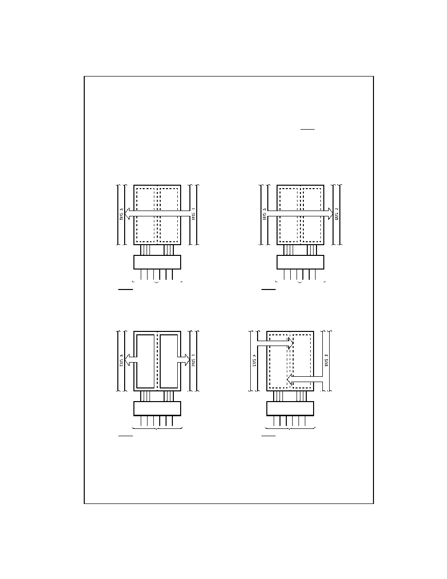
Functional Description
In the transceiver mode, data present at the HIGH imped-
ance port may be stored in either the A or B register or
both.
The select (SAB
n
, SBA
n
) controls can multiplex stored and
real-time.
The examples below demonstrate the four fundamental
bus-management functions that can be performed with the
74LCX32652 for data register I/O 1A and 1B: 0 - 7.
Data on the A or B data bus, or both can be stored in the
internal D flip-flop by LOW-to-HIGH transitions at the
appropriate Clock Inputs (CPAB
n
, CPBA
n
) regardless of
the Select or Output Enable Inputs. When SAB and SBA
are in the real time transfer mode, it is also possible to
store data without using the internal D flip-flops by simulta-
neously enabling OEAB
n
and OEBA
n
. In this configuration
each Output reinforces its Input. Thus when all other data
sources to the two sets of bus lines are in a HIGH imped-
ance state, each set of bus lines will remain at its last state.
Real-Time
Transfer Bus B to Bus A
Real-Time
Transfer Bus A to Bus B
OEAB
1
OEBA
1
CPAB
1
CPBA
1
SAB
1
SBA
1
OEAB
1
OEBA
1
CPAB
1
CPBA
1
SAB
1
SBA
1
L
L
X
X
X
L
H
H
X
X
L
X
Transfer Storage
Data to A or B
Storage
OEAB
1
OEBA
1
CPAB
1
CPBA
1
SAB
1
SBA
1
OEAB
1
OEBA
1
CPAB
1
CPBA
1
SAB
1
SBA
1
H
L
H or L
H or L
H
H
X
H
X
X
X
L
X
X
X
X
L
H
X
X

