
© 2005 Fairchild Semiconductor Corporation
DS011995
www.fairchildsemi.com
February 1994
Revised October 2005
7
4
LC
X3
73
Low
V
o
lt
a
g
e O
c
t
a
l T
r
ans
p
a
r
ent
La
tc
h with 5V T
o
l
e
rant
I
npu
t
s
and Output
s
74LCX373
Low Voltage Octal Transparent Latch
with 5V Tolerant Inputs and Outputs
General Description
The LCX373 consists of eight latches with 3-STATE outputs for
bus organized system applications. The device is designed for
low voltage (3.3V or 2.5V) V
CC
applications with capability of
interfacing to a 5V signal environment.
The LCX373 is fabricated with an advanced CMOS technology
to achieve high speed operation while maintaining CMOS low
power dissipation.
Features
O
5V tolerant inputs and outputs
O
2.3V≠3.6V V
CC
specifications provided
O
8.0 ns t
PD
max (V
CC
3.3V), 10
P
A I
CC
max
O
Power-down high impedance inputs and outputs
O
Supports live insertion/withdrawal (Note )
O r
24 mA output drive (V
CC
3.0V)
O
Implements patented noise/EMI reduction circuitry
O
Latch-up performance exceeds JEDEC 78 conditions
O
ESD performance:
Human Body Model
!
2000V
Machine Model
!
200V
O
Leadless Pb-Free DQFN package
Note 1: To ensure the high-impedance state during power up or down, OE should be
tied to V
CC
through a pull-up resistor: the minimum value or the resistor is determined
by the current-sourcing capability of the driver.
Ordering Code:
Devices also available in Tape and Reel. Specify by appending suffix letter "X" to the ordering code.
Pb-Free package per JEDEC J-STD-020B.
Note 2: DQFN package available in Tape and Reel only.
Note 3: "_NL" indicates Pb-Free package (per JEDEC J-STD-020B). Device available in Tape and Reel only.
Order Number
Package
Package Description
Number
74LCX373WM
M20B
20-Lead Small Outline Integrated Circuit (SOIC), JEDEC MS-013, 0.300" Wide
74LCX373SJ
M20D
Pb-Free 20-Lead Small Outline Package (SOP), EIAJ TYPE II, 5.3mm Wide
74LCX373BQX
(Preliminary)
(Note 2)
MLP020B
Pb-Free 20-Terminal Depopulated Quad Very-Thin Flat Pack No Leads (DQFN), JEDEC
MO-241, 2.5 x 4.5mm
74LCX373MSA
MSA20
20-Lead Shrink Small Outline Package (SSOP), JEDEC MO-150, 5.3mm Wide
74LCX373MTC
MTC20
20-Lead Thin Shrink Small Outline Package (TSSOP), JEDEC MO-153, 4.4mm Wide
74LCX373MTCX_NL
(Note 3)
MTC20
Pb-Free 20-Lead Thin Shrink Small Outline Package (TSSOP), JEDEC MO-153, 4.4mm
Wide
www.fairchildsemi.com
2
74LC
X
373
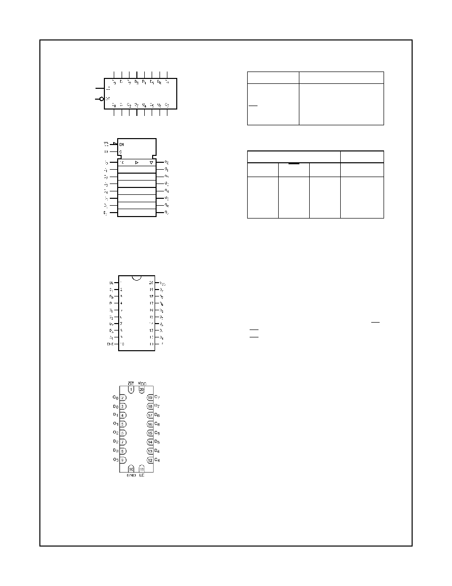
Logic Symbols
IEEE/IEC
Connection Diagrams
Pin Assignments for
SOIC, SOP, SSOP, TSSOP
Pad Assignments for DQFN
(Top View)
Pin Descriptions
Truth Table
H
HIGH Voltage Level
L
LOW Voltage Level
Z
High Impedance
X
Immaterial
O
0
Previous O
0
before HIGH-to-LOW transition of Latch Enable
Functional Description
The LCX373 contains eight D-type latches with 3-STATE stan-
dard outputs. When the Latch Enable (LE) input is HIGH, data
on the D
n
inputs enters the latches. In this condition the latches
are transparent, i.e. a latch output will change state each time
its D input changes. When LE is LOW, the latches store the
information that was present on the D inputs a setup time pre-
ceding the HIGH-to-LOW transition of LE. The 3-STATE stan-
dard outputs are controlled by the Output Enable (OE) input.
When OE is LOW, the standard outputs are in the 2-state mode.
When OE is HIGH, the standard outputs are in the high imped-
ance mode but this does not interfere with entering new data
into the latches.
Pin Names
Description
D
0
≠D
7
Data Inputs
LE
Latch Enable Input
OE
Output Enable Input
O
0
≠O
7
3-STATE Latch Outputs
Inputs
Outputs
LE
OE
D
n
O
n
X
H
X
Z
H
L
L
L
H
L
H
H
L
L
X
O
0

www.fairchildsemi.com
4
74LC
X
373
Absolute Maximum Ratings
(Note 4)
Recommended Operating Conditions
(Note 6)
Note 4: The Absolute Maximum Ratings are those values beyond which the safety of the device cannot be guaranteed. The device should not be operated at these limits. The
parametric values defined in the Electrical Characteristics tables are not guaranteed at the Absolute Maximum Ratings. The "Recommended Operating Conditions" table will
define the conditions for actual device operation.
Note 5: I
O
Absolute Maximum Rating must be observed.
Note 6: Unused inputs must be held HIGH or LOW. They may not float.
DC Electrical Characteristics
Symbol
Parameter
Value
Conditions
Units
V
CC
Supply Voltage
0.5 to
7.0
V
V
I
DC Input Voltage
0.5 to
7.0
V
V
O
DC Output Voltage
0.5 to
7.0
Output in 3-STATE
V
0.5 to V
CC
0.5 Output in HIGH or LOW State (Note 5)
I
IK
DC Input Diode Current
50
V
I
GND
mA
I
OK
DC Output Diode Current
50
V
O
GND
mA
50
V
O
!
V
CC
I
O
DC Output Source/Sink Current
r
50
mA
I
CC
DC Supply Current per Supply Pin
r
100
mA
I
GND
DC Ground Current per Ground Pin
r
100
mA
T
STG
Storage Temperature
65 to
150
q
C
Symbol
Parameter
Min
Max
Units
V
CC
Supply Voltage
Operating
2.0
3.6
V
Data Retention
1.5
3.6
V
I
Input Voltage
0
5.5
V
V
O
Output Voltage
HIGH or LOW State
0
V
CC
V
3-STATE
0
5.5
I
OH
/I
OL
Output Current
V
CC
3.0V
3.6V
r
24
mA
V
CC
2.7V
3.0V
r
12
V
CC
2.3V
2.7V
r
8
T
A
Free-Air Operating Temperature
40
85
q
C
'
t/
'
V
Input Edge Rate, V
IN
0.8V
2.0V, V
CC
3.0V
0
10
ns/V
Symbol
Parameter
Conditions
V
CC
T
A
40
q
C to
85
q
C
Units
(V)
Min
Max
V
IH
HIGH Level Input Voltage
2.3
2.7
1.7
V
2.7
3.6
2.0
V
IL
LOW Level Input Voltage
2.3
2.7
0.7
V
2.7
3.6
0.8
V
OH
HIGH Level Output Voltage
I
OH
100
P
A
2.3
3.6
V
CC
0.2
V
I
OH
8 mA
2.3
1.8
I
OH
12 mA
2.7
2.2
I
OH
18 mA
3.0
2.4
I
OH
24 mA
3.0
2.2
V
OL
LOW Level Output Voltage
I
OL
100
P
A
2.3
3.6
0.2
V
I
OL
8 mA
2.3
0.6
I
OL
12 mA
2.7
0.4
I
OL
16 mA
3.0
0.4
I
OL
24 mA
3.0
0.55
I
I
Input Leakage Current
0
d
V
I
d
5.5V
2.3
3.6
r
5.0
P
A
I
OZ
3-STATE Output Leakage
0
d
V
O
d
5.5V
2.3
3.6
r
5.0
P
A
V
I
V
IH
or V
IL
I
OFF
Power-Off Leakage Current
V
I
or V
O
5.5V
0
10
P
A
I
CC
Quiescent Supply Current
V
I
V
CC
or GND
2.3
3.6
10
P
A
3.6V
d
V
I
, V
O
d
5.5V (Note 7)
2.3
3.6
r
10

5
www.fairchildsemi.com
74
LCX
3
7
3
DC Electrical Characteristics
(Continued)
Note 7: Outputs disabled or 3-STATE only.
AC Electrical Characteristics
Note 8: Skew is defined as the absolute value of the difference between the actual propagation delay for any two separate outputs of the same device. The specification applies
to any outputs switching in the same direction, either HIGH-to-LOW (t
OSHL
) or LOW-to-HIGH (t
OSLH
).
Dynamic Switching Characteristics
Capacitance
Symbol
Parameter
Conditions
V
CC
T
A
40
q
C to
85
q
C
Units
(V)
Min
Max
'
I
CC
Increase in I
CC
per Input
V
IH
V
CC
0.6V
2.3
3.6
500
P
A
Symbol
Parameter
T
A
40
q
C to
85
q
C, R
L
500
:
Units
V
CC
3.3V
r
0.3V
V
CC
2.7V
V
CC
2.5V
r
0.2V
C
L
50pF
C
L
50pF
C
L
30pF
Min
Max
Min
Max
Min
Max
t
PHL
Propagation Delay
1.5
8.0
1.5
9.0
1.5
9.6
ns
t
PLH
D
n
to O
n
1.5
8.0
1.5
9.0
1.5
9.6
t
PHL
Propagation Delay
1.5
8.5
1.5
9.5
1.5
10.5
ns
t
PLH
LE to O
n
1.5
8.5
1.5
9.5
1.5
10.5
t
PZL
Output Enable Time
1.5
8.5
1.5
9.5
1.5
10.5
ns
t
PZH
1.5
8.5
1.5
9.5
1.5
10.5
t
PLZ
Output Disable Time
1.5
7.5
1.5
8.5
1.5
9.0
ns
t
PHZ
1.5
7.5
1.5
8.5
1.5
9.0
t
S
Setup Time, D
n
to LE
2.5
2.5
4.0
ns
t
H
Hold Time, D
n
to LE
1.5
1.5
2.0
ns
t
W
LE Pulse Width
3.3
3.3
4.0
ns
t
OSHL
Output to Output Skew
1.0
ns
t
OSLH
(Note 8)
1.0
Symbol
Parameter
Conditions
V
CC
T
A
25
q
C
Units
(V)
Typical
V
OLP
Quiet Output Dynamic Peak V
OL
C
L
50 pF, V
IH
3.3V, V
IL
0V
3.3
0.8
V
C
L
30pF, V
I
2.5V, V
IL
0V
2.5
0.6
V
OLV
Quiet Output Dynamic Valley V
OL
C
L
50 pF, V
IH
3.3V, V
IL
0V
3.3
0.8
V
C
L
30pF, V
I
2.5V, V
IL
0V
2.5
0.6
Symbol
Parameter
Conditions
Typical
Units
C
IN
Input Capacitance
V
CC
Open, V
I
0V or V
CC
7
pF
C
OUT
Output Capacitance
V
CC
3.3V, V
I
0V or V
CC
8
pF
C
PD
Power Dissipation Capacitance
V
CC
3.3V, V
I
0V or V
CC
, f
10 MHz
25
pF
