©2006 Fairchild Semiconductor Corporation
1
www.fairchildsemi.com
February 2006
74LCX541 Rev. 2.0.0
74LCX541 Lo
w
V
olta
g
e
Octal Buff
er/Line Driver with 5V
T
olerant Inputs and Outputs
74LCX541
Low Voltage Octal Buffer/Line Driver
with 5V Tolerant Inputs and Outputs
Features
5V tolerant input and outputs
2.3V3.6V V
CC
specifications provided
6.5ns t
PD
max (V
CC
=
3.3V), 10
µ
A I
CC
max
Power-down high impedance inputs and outputs
Supports live insertion/withdrawal
1
±
24 mA output drive (V
CC
=
3.0V)
Implements patented noise/ EMI reduction circuitry
Latch-up performance exceeds JEDEC 78 conditions
ESD performance
Human body model
>
2000V
Machine model
>
200V
Leadless Pb-Free DQFN package
General Description
The LCX541 is an octal buffer/line driver designed to be
employed as memory and address drivers, clock drivers
and bus oriented transmitter/receivers. The LCX541 is a
non inverting option of the LCX540.
This device is similar in function to the LCX244 while
providing flow-through architecture (inputs on opposite
side from outputs). This pinout arrangement makes this
device especially useful as an output port for micropro-
cessors, allowing ease of layout and greater PC board
density.
The LCX541 is designed for low voltage applications
with capability of interfacing to a 5V signal environment.
The LCX541 is fabricated with an advanced CMOS
technology to achieve high speed operation while
maintaining CMOS low power dissipation.
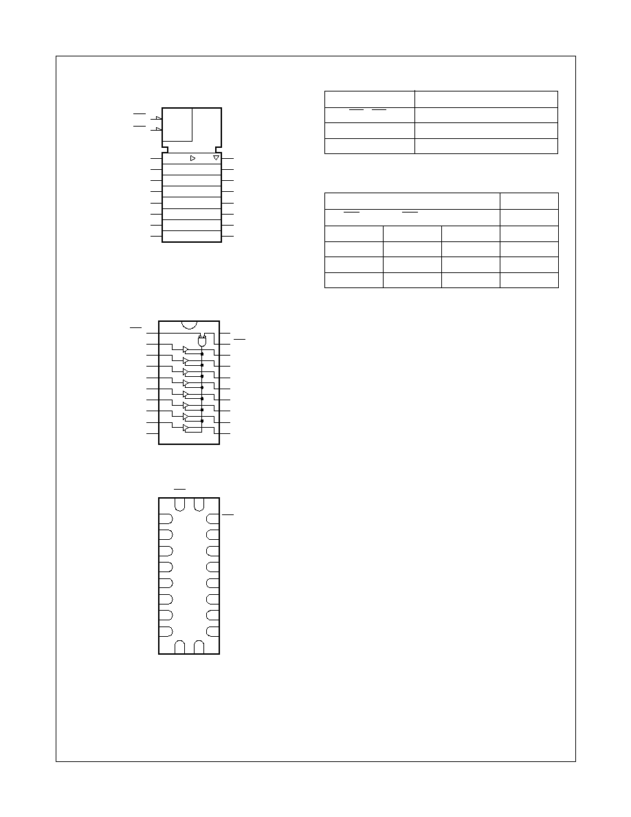
Ordering Information
Devices also available in Tape and Reel. Specify by appending the suffix letter "X" to the ordering code.
Pb-Free package per JEDED J-STD-020B.
Notes:
1.
To ensure the high impedance state during power up or down, OE should be tied to V
CC
through a pull-up resistor: the minimum
value of the resistor is determined by the current-sourcing capability of the driver.
2.
DQFN package available in Tape and Reel only.
3.
"_NL" indicates Pb-Free package (per JEDEC J-STD-020B). Device available in Tape and Reel only.
Order Number
Package
Number
Package Description
74LCX541WM
M20B
20-Lead Small Outline Integrated Circuit (SOIC), JEDEC MS-013, 0.300" Wide
74LCX541SJ
M20D
20-Lead Small Outline Package (SOP), EIAJ TYPE II, 5.3mm Wide
74LCX541BQX
2
MLP020B
Pb-Free 20-Terminal Depopulated Quad Very-Thin Flat Pack No Leads (DQFN),
JEDEC MO-241, 2.5 x 4.5mm
74LCX541MSA
MSA20
20-Lead Shrink Small Outline Package (SSOP), JEDEC MO-150, 5.3mm Wide
74LCX541MTC
MTC20
20-Lead Thin Shrink Small Outline Package (TSSOP), JEDEC MO-153,
4.4mm Wide
74LCX541MTC_NL
3
MTC20
Pb-Free 20-Lead Thin Shrink Small Outline Package (TSSOP), JEDEC
MO-153, 4.4mm Wide
3
www.fairchildsemi.com
74LCX541 Rev. 2.0.0
74LCX541 Lo
w
V
olta
g
e
Octal Buff
er/Line Driver with 5V
T
olerant Inputs and Outputs
Absolute Maximum Ratings
The Absolute Maximum Ratings are those values beyond which the safety of the device cannot be guaranteed. The
device should not be operated at these limits. The parametric values defined in the Electrical Characteristics tables are
not guaranteed at the Absolute Maximum Ratings. The "Recommended Operating Conditions" table will define the
conditions for actual device operation.
Recommended Operating Conditions
5
Notes:
4.
I
O
Absolute Maximum Rating must be observed.
5.
Unused inputs or I/O's must be held HIGH or LOW. They may not float.
Symbol
Parameter
Conditions
Value
Units
V
CC
Supply Voltage
-
0.5 to
+
7.0
V
V
I
DC Input Voltage
-
0.5 to
+
7.0
V
V
O
DC Output Voltage
Output in 3-STATE
-
0.5 to
+
7.0
V
Output in HIGH or LOW State
4
-
0.5 to V
CC
+
0.5
I
IK
DC Input Diode Current
V
I
<
GND
-
50
mA
I
OK
DC Output Diode Current
V
O
<
GND
-
50
mA
V
O
>
V
CC
+
50
I
O
DC Output Source/Sink Current
±
50
mA
I
CC
DC Supply Current per Supply Pin
±
100
mA
I
GND
DC Ground Current per Ground Pin
±
100
mA
T
STG
Storage Temperature
-
65 to
+
150
°
C
Symbol
Parameter
Conditions
Min.
Max.
Units
V
CC
Supply Voltage
Operating
2.0
3.6
V
Data Retention
1.5
3.6
V
I
Input Voltage
0
5.5
V
V
O
Output Voltage
HIGH or LOW State
0
V
CC
V
3-STATE
0
5.5
I
OH
/
I
OL
Output Current
V
CC
=
3.0V
-
3.6V
±
24
mA
V
CC
=
2.7V
-
3.0V
±
12
V
CC
=
2.3V
-
2.7V
±
8
T
A
Free-Air Operating Temperature
-
40
85
°
C
t
/
V
Input Edge Rate
V
IN
=
0.8V 2.0V, V
CC
=
3.0V
0
10
ns
/
V
4
www.fairchildsemi.com
74LCX541 Rev. 2.0.0
74LCX541 Lo
w
V
olta
g
e
Octal Buff
er/Line Driver with 5V
T
olerant Inputs and Outputs
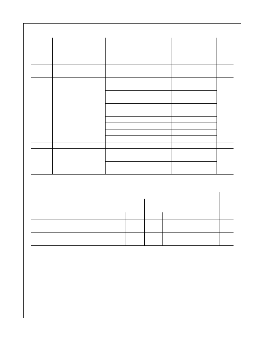
DC Electrical Characteristics
AC Electrical Characteristics
Notes
6.
Outputs disabled or 3-STATE only.
7.
Skew is defined as the absolute value of the difference between the actual propagation delay for any two separate outputs of the
same device. The specification applies to any outputs switching in the same direction, either HIGH-to-LOW (t
OSHL
) or LOW-to-
HIGH (t
OSLH
).
Symbol
Parameter
Conditions
V
CC
(V)
T
A
=
-
40
°
C to
+
85
°
C
Units
Min.
Max.
V
IH
HIGH Level Input Voltage
2.3
-
2.7
1.7
V
2.7
-
3.6
2.0
V
IL
LOW Level Input Voltage
2.3
-
2.7
0.7
V
2.7
-
3.6
0.8
V
OH
HIGH Level Output Voltage
I
OH
=
-
100
µ
A
2.3
-
3.6
V
CC
0.2
V
I
OH
= 8 mA
2.3
1.8
I
OH
=
-
12 mA
2.7
2.2
I
OH
=
-
18 mA
3.0
2.4
I
OH
=
-
24 mA
3.0
2.2
V
OL
LOW Level Output Voltage
I
OL
=
100
µ
A
2.3
-
3.6
0.2
V
I
OL
= 8mA
2.3
0.6
I
OL
=
12 mA
2.7
0.4
I
OL
=
16 mA
3.0
0.4
I
OL
=
24 mA
3.0
0.55
I
I
Input Leakage Current
0
V
I
5.5V
2.3
-
3.6
±
5.0
µ
A
I
OFF
Power-Off Leakage Current
V
I
or V
O
=
5.5V
0
10
µ
A
I
CC
Quiescent Supply Current
V
I
=
V
CC
or GND
2.3
-
3.6
10
µ
A
3.6V
V
I
, V
O
5.5V
6
2.3
-
3.6
±
10
I
CC
Increase in I
CC
per Input
V
IH
=
V
CC
=
0.6V
2.3
-
3.6
500
µ
A
Symbol
Parameter
T
A
=
-
40
°
C to
+
85
°
C, R
L
=
500
Units
V
CC
=
3.3V
±
0.3V
V
CC
=
2.7V
V
CC
=
2.5V
±
0.2V
C
L
=
50pF
C
L
=
50pF
C
L
=
30pF
Min.
Max.
Min.
Max.
Min.
Max.
t
PHL
, t
PLH
Propagation Delay
1.5
6.5
1.5
7.5
1.5
7.8
ns
t
PZL
, t
PZH
Output Enable Time
1.5
8.5
1.5
9.5
1.5
10.5
ns
t
PLZ
, t
PHZ
Output Disable Time
1.5
7.5
1.5
8.5
1.5
9.0
ns
t
OSHL
, t
OSLH
Output to Output Skew
7
1.0
ns