
© 2002 Fairchild Semiconductor Corporation
DS500580
www.fairchildsemi.com
March 2002
Revised March 2002
7
4
LCXZ16245 Low
V
o
lt
age 16-Bi
t Bidi
rect
i
onal T
r
ans
ceiver
wi
th 5V
T
o
l
e
ran
t
Input
s
a
nd
Out
puts
74LCXZ16245
Low Voltage 16-Bit Bidirectional Transceiver
with 5V Tolerant Inputs and Outputs
General Description
The LCXZ16245 contains sixteen non-inverting bidirec-
tional buffers with 3-STATE outputs and is intended for bus
oriented applications. The device is designed for low volt-
age (2.7V or 3.3V) V
CC
applications with capability of inter-
facing to a 5V signal environment. The device is byte
controlled. Each byte has separate control inputs which
could be shorted together for full 16-bit operation. The T/R
inputs determine the direction of data flow through the
device. The OE inputs disable both the A and B ports by
placing them in a high impedance state.
When V
CC
is between 0V and 1.5V, the LCXZ16245 is on
the high impedance state during power-up or power-down.
This places the outputs in the high impedance (Z) state
preventing intermittent low impedance loading or glitching
in bus oriented applications.
The LCXZ16245 is fabricated with an advanced CMOS
technology to achieve high speed operation while maintain-
ing CMOS low power dissipation.
Features
s
5V tolerant inputs and outputs
s
2.7V≠3.6V V
CC
specifications provided
s
4.5 ns t
PD
max (V
CC
=
3.3V), 20
µ
A I
CC
max
s
Power-down high impedance inputs and outputs
s
Supports live insertion/withdrawal (Note 1)
s
±
24 mA output drive (V
CC
=
3.0V)
s
Implements patented noise/EMI reduction circuitry
s
Latch-up performance conforms to the requirements of
JESD78
s
ESD performance:
Human body model
>
2000V
Machine model
>
200V
s
Also packaged in plastic Fine-Pitch Ball Grid Array
(FBGA) (Preliminary)
Note 1: To ensure the high-impedance state during power up or down, OE
should be tied to V
CC
through a pull-up resistor: the minimum value or the
resistor is determined by the current-sourcing capability of the driver.
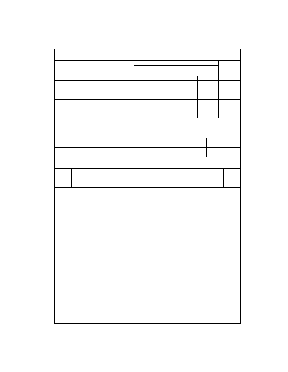
Ordering Code:
Devices also available in Tape and Reel. Specify by appending the suffix letter "X" to the ordering code.
Note 2: BGA package available in Tape and Reel only.
Logic Symbol
Order Number
Package Number
Package Description
74LCXZ16245GX
(Note 2)
BGA54A
(Preliminary)
54-Ball Fine-Pitch Ball Grid Array (FBGA), JEDEC MO-205, 5.5mm Wide
[TAPE and REEL]
74LCXZ16245MTD
MTD48
48-Lead Thin Shrink Small Outline Package (TSSOP), JEDEC MO-153, 6.1mm Wide

www.fairchildsemi.com
2
74LCXZ16245
Connection Diagrams
Pin Assignment for SSOP and TSSOP
Pin Assignment for FBGA
(Top Thru View)
Pin Descriptions
FBGA Pin Assignments
Truth Tables
H
=
HIGH Voltage Level
L
=
LOW Voltage Level
X
=
Immaterial
Z
=
High Impedance
Logic Diagram
Pin Names
Description
OE
n
Output Enable Input
T/R
n
Transmit/Receive Input
A
0
≠A
15
Side A Inputs or 3-STATE Outputs
B
0
≠B
15
Side B Inputs or 3-STATE Outputs
NC
No Connect
1
2
3
4
5
6
A
B
0
NC
T/R
1
OE
1
NC
A
0
B
B
2
B
1
NC
NC
A
1
A
2
C
B
4
B
3
V
CC
V
CC
A
3
A
4
H
B
6
B
5
GND
GND
A
5
A
6
E
B
8
B
7
GND
GND
A
7
A
8
F
B
10
B
9
GND
GND
A
9
A
10
G
B
12
B
11
V
CC
V
CC
A
11
A
12
H
B
14
B
13
NC
NC
A
13
A
14
J
B
15
NC
T/R
2
OE
2
NC
A
15
Inputs
Outputs
OE
1
T/R
1
L
L
Bus B
0
≠B
7
Data to Bus A
0
≠A
7
L
H
Bus A
0
≠A
7
Data to Bus B
0
≠B
7
H
X
HIGH Z State on A
0
≠A
7
, B
0
≠B
7
Inputs
Outputs
OE
2
T/R
2
L
L
Bus B
8
≠B
15
Data to Bus A
8
≠A
15
L
H
Bus A
8
≠A
15
Data to Bus B
8
≠B
15
H
X
HIGH Z State on A
8
≠A
15
, B
8
≠B
15

3
www.fairchildsemi.com
7
4
LCXZ16245
Absolute Maximum Ratings
(Note 3)
Recommended Operating Conditions
(Note 5)
Note 3: The Absolute Maximum Ratings are those values beyond which the safety of the device cannot be guaranteed. The device should not be operated
at these limits. The parametric values defined in the Electrical Characteristics tables are not guaranteed at the Absolute Maximum Ratings. The "Recom-
mended Operating Conditions" table will define the conditions for actual device operation.
Note 4: I
O
Absolute Maximum Rating must be observed.
Note 5: Unused inputs or I/O's must be held HIGH or LOW. They may not float.
DC Electrical Characteristics
Note 6: Outputs disabled or 3-STATE only.
Symbol
Parameter
Value
Conditions
Units
V
CC
Supply Voltage
-
0.5 to
+
7.0
V
V
I
DC Input Voltage
-
0.5 to
+
7.0
V
V
O
DC Output Voltage
-
0.5 to
+
7.0
Output in 3-STATE
V
-
0.5 to V
CC
+
0.5
Output in HIGH or LOW State (Note 4)
I
IK
DC Input Diode Current
-
50
V
I
<
GND
mA
I
OK
DC Output Diode Current
-
50
V
O
<
GND
mA
+
50
V
O
>
V
CC
I
O
DC Output Source/Sink Current
±
50
mA
I
CC
DC Supply Current per Supply Pin
±
100
mA
I
GND
DC Ground Current per Ground Pin
±
100
mA
T
STG
Storage Temperature
-
65 to
+
150
∞
C
Symbol
Parameter
Min
Max
Units
V
CC
Supply Voltage
Operating
2.7
3.6
V
V
I
Input Voltage
0
5.5
V
V
O
Output Voltage
HIGH or LOW State
0
V
CC
V
3-STATE
0
5.5
I
OH
/I
OL
Output Current
V
CC
=
3.0V
-
3.6V
±
24
mA
V
CC
=
2.7V
-
3.0V
±
12
T
A
Free-Air Operating Temperature
-
40
85
∞
C
t/
V
Input Edge Rate, V
IN
=
0.8V≠2.0V, V
CC
=
3.0V
0
10
ns/V
Symbol
Parameter
Conditions
V
CC
T
A
=
-
40
∞
C to
+
85
∞
C
Units
(V)
Min
Max
V
IH
HIGH Level Input Voltage
2.7
-
3.6
2.0
V
V
IL
LOW Level Input Voltage
2.7
-
3.6
0.8
V
V
OH
HIGH Level Output Voltage
I
OH
=
-
100
µ
A
2.7
-
3.6
V
CC
-
0.2
V
I
OH
=
-
12 mA
2.7
2.2
I
OH
=
-
18 mA
3.0
2.4
I
OH
=
-
24 mA
3.0
2.2
V
OL
LOW Level Output Voltage
I
OL
=
100
µ
A
2.7
-
3.6
0.2
V
I
OL
=
12 mA
2.7
0.4
I
OL
=
16 mA
3.0
0.4
I
OL
=
24 mA
3.0
0.55
I
I
Input Leakage Current
0
V
I
5.5V
2.7
-
3.6
±
5.0
µ
A
I
OZ
3-STATE I/O Leakage
0
V
O
5.5V
2.7
-
3.6
±
5.0
µ
A
V
I
=
V
IH
or V
IL
I
OFF
Power-Off Leakage Current
V
I
or V
O
=
5.5V
0
10
µ
A
I
PU/PD
Power-Up/Power-Down V
O
=
0.5V to V
CC
0 - 1.5
±
5.0
µ
A
3-STATE Output Current
V
I
=
V
CC
or GND
I
CC
Quiescent Supply Current
V
I
=
V
CC
or GND
2.7≠3.6
225
µ
A
3.6V
V
I
, V
O
5.5V (Note 6)
2.7≠3.6
±
225
I
CC
Increase in I
CC
per Input
V
IH
=
V
CC
-
0.6V
2.7≠3.6
500
µ
A
www.fairchildsemi.com
4
74LCXZ16245
AC Electrical Characteristics
Note 7: Skew is defined as the absolute value of the difference between the actual propagation delay for any two separate outputs of the same device. The
specification applies to any outputs switching in the same direction, either HIGH-to-LOW (t
OSHL
) or LOW-to-HIGH (t
OSLH
). Parameter guaranteed by design.
Dynamic Switching Characteristics
Capacitance
Symbol
Parameter
T
A
=
-
40
∞
C to
+
85
∞
C, R
L
=
500
Units
V
CC
=
3.3V
±
0.3V
V
CC
=
2.7V
C
L
=
50 pF
C
L
=
50 pF
Min
Max
Min
Max
t
PHL
Propagation Delay
1.0
4.5
1.0
5.2
ns
t
PLH
A
n
to B
n
or B
n
to A
n
1.0
4.5
1.0
5.2
t
PZL
Output Enable Time
1.0
6.5
1.0
7.2
ns
t
PZH
1.0
6.5
1.0
7.2
t
PLZ
Output Disable Time
1.0
6.4
1.0
6.9
ns
t
PHZ
1.0
6.4
1.0
6.9
t
OSHL
Output to Output Skew (Note 7)
1.0
ns
t
OSLH
1.0
Symbol
Parameter
Conditions
V
CC
T
A
=
25
∞
C
Units
(V)
Typical
V
OLP
Quiet Output Dynamic Peak V
OL
C
L
=
50 pF, V
IH
=
3.3V, V
IL
=
0V
3.3
0.8
V
V
OLV
Quiet Output Dynamic Valley V
OL
C
L
=
50 pF, V
IH
=
3.3V, V
IL
=
0V
3.3
-
0.8
V
Symbol
Parameter
Conditions
Typical
Units
C
IN
Input Capacitance
V
CC
=
Open, V
I
=
0V or V
CC
7
pF
C
I/O
Input/Output Capacitance
V
CC
=
3.3V, V
I
=
0V or V
CC
8
pF
C
PD
Power Dissipation Capacitance
V
CC
=
3.3V, V
I
=
0V or V
CC
, f
=
10 MHz
20
pF

5
www.fairchildsemi.com
7
4
LCXZ16245
AC LOADING and WAVEFORMS
Generic for LCX Family
FIGURE 1. AC Test Circuit (C
L
includes probe and jig capacitance)
Waveform for Inverting and Non-Inverting Functions
Propagation Delay. Pulse Width and t
rec
Waveforms
3-STATE Output Low Enable and
Disable Times for Logic
3-STATE Output High Enable and
Disable Times for Logic
Setup Time, Hold Time and Recovery Time for Logic
t
rise
and t
fall
FIGURE 2. Waveforms
(Input Characteristics; f =1MHz, t
r
= t
f
= 3ns)
Test
Switch
t
PLH
, t
PHL
Open
t
PZL
, t
PLZ
6V at V
CC
=
3.3
±
0.3V, and 2.7V
t
PZH
, t
PHZ
GND
Symbol
V
CC
3.3V
±
0.3V
2.7V
V
mi
1.5V
1.5V
V
mo
1.5V
1.5V
V
x
V
OL
+
0.3V
V
OL
+
0.3V
V
y
V
OH
-
0.3V
V
OH
-
0.3V
www.fairchildsemi.com
6
74LCXZ16245
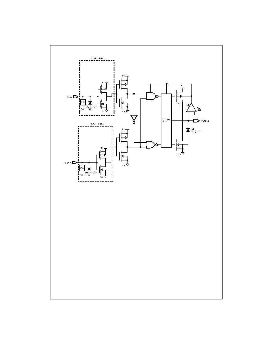
Schematic Diagram
Generic for LCX Family

7
www.fairchildsemi.com
7
4
LCXZ16245
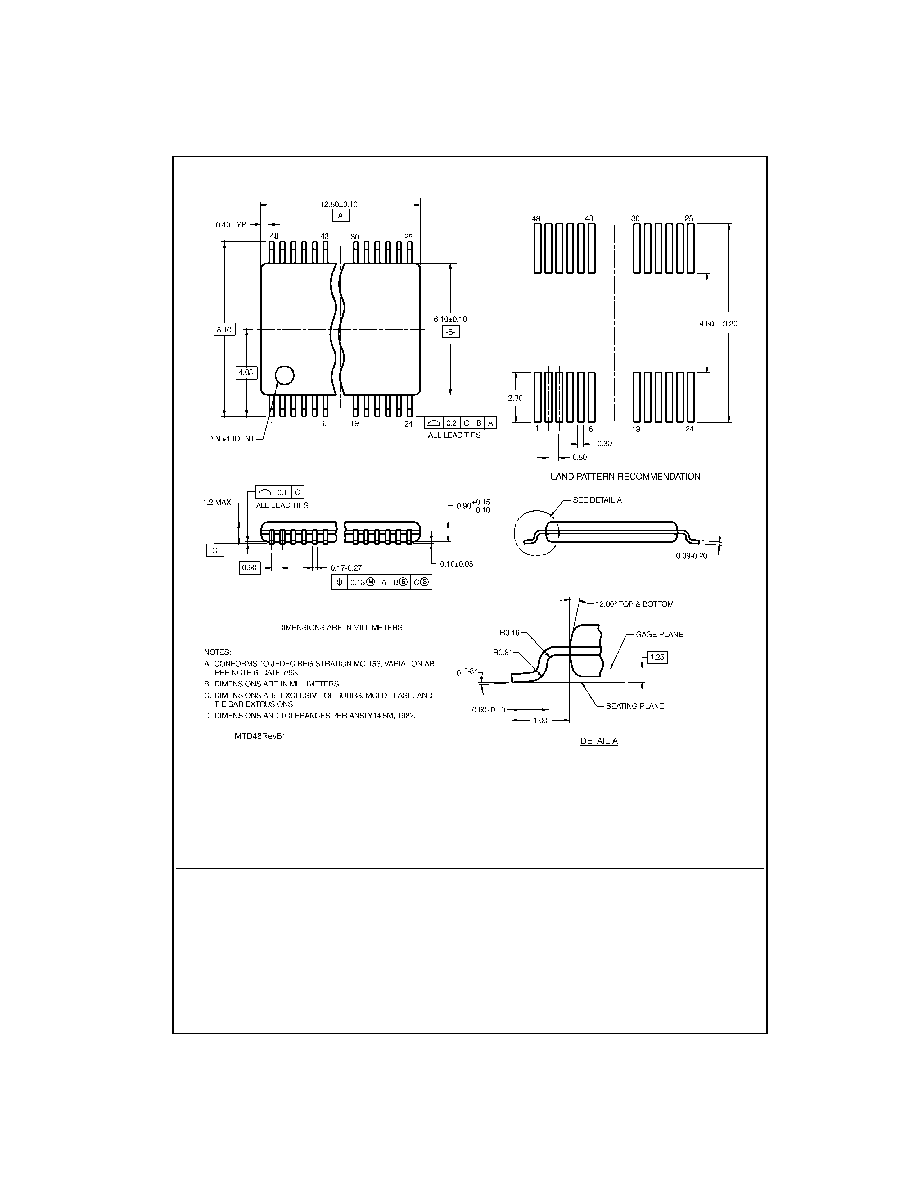
Physical Dimensions
inches (millimeters) unless otherwise noted
54-Ball Fine-Pitch Ball Grid Array (FBGA), JEDEC MO-205, 5.5mm Wide
Package Number BGA54A
Preliminary
www.fairchildsemi.com
8
74LCXZ16245 Low
V
o
l
t
age 16-
Bit
Bi
dir
ecti
onal
T
r
anscei
ver w
i
t
h
5V T
o
ler
ant Inp
u
ts and O
u
t
puts
Physical Dimensions
inches (millimeters) unless otherwise noted (Continued)
48-Lead Thin Shrink Small Outline Package (TSSOP), JEDEC MO-153, 6.1mm Wide
Package Number MTD48
Fairchild does not assume any responsibility for use of any circuitry described, no circuit patent licenses are implied and
Fairchild reserves the right at any time without notice to change said circuitry and specifications.
LIFE SUPPORT POLICY
FAIRCHILD'S PRODUCTS ARE NOT AUTHORIZED FOR USE AS CRITICAL COMPONENTS IN LIFE SUPPORT
DEVICES OR SYSTEMS WITHOUT THE EXPRESS WRITTEN APPROVAL OF THE PRESIDENT OF FAIRCHILD
SEMICONDUCTOR CORPORATION. As used herein:
1. Life support devices or systems are devices or systems
which, (a) are intended for surgical implant into the
body, or (b) support or sustain life, and (c) whose failure
to perform when properly used in accordance with
instructions for use provided in the labeling, can be rea-
sonably expected to result in a significant injury to the
user.
2. A critical component in any component of a life support
device or system whose failure to perform can be rea-
sonably expected to cause the failure of the life support
device or system, or to affect its safety or effectiveness.
www.fairchildsemi.com