© 2000 Fairchild Semiconductor Corporation
DS500410
www.fairchildsemi.com
October 2000
Revised October 2000
7
4
LCXZ2245
L
o
w
V
o
lt
age B
i
di
rect
ional
T
r
anscei
ver
wit
h
5V
T
o
l
e
rant
I
nput
s
and Output
s and
26
Seri
es
Res
i
st
ors in B
Out
puts
74LCXZ2245
Low Voltage Bidirectional Transceiver
with 5V Tolerant Inputs and Outputs
and 26
Series Resistors in B Outputs
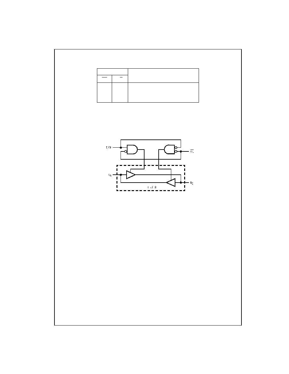
General Description
The LCXZ2245 contains eight non-inverting bidirectional
buffers with 3-STATE outputs and is intended for bus ori-
ented applications. The device is designed for low voltage
(2.7V and 3.3V) V
CC
applications with capability of interfac-
ing to a 5V signal environment. The T/R input determines
the direction of data flow through the device. The OE input
disables both the A and B ports by placing them in a high
impedance state. The 26
series resistor in the B Port out-
put helps reduce output overshoot and undershoot.
The LCXZ2245 is fabricated with an advanced CMOS
technology to achieve high speed operation while maintain-
ing CMOS low power dissipation.
When V
CC
is between 0 and 1.5V, the LCXZ2245 is on the
high impedance state during power up or power down. This
places the outputs in the high impedance (Z) state prevent-
ing intermittent low impedance loading or glitching in bus
oriented applications.
Features
s
5V tolerant inputs and outputs
s
2.7V≠3.6V V
CC
specifications provided
s
7.0 ns t
PD
max (V
CC
=
3.3V), 10
µ
A I
CC
max
s
Power down high impedance inputs and outputs
s
Supports live insertion/withdrawal (Note 1)
s
±
12 mA output drive on the B Port (V
CC
=
3.0V)
s
Implements patented noise/EMI reduction circuitry
s
Latch-up performance exceeds 500 mA
s
Equivalent 26
series resistor on all B Port outputs
s
ESD performance:
Human body model
>
2000V
Machine model
>
200V
Note 1: To ensure the high-impedance state during power up or down, OE
should be tied to V
CC
through a pull-up resistor: the minimum value or the
resistor is determined by the current-sourcing capability of the driver.
Ordering Code:
Devices also available in Tape and Reel. Specify by appending the suffix letter "X" to the ordering code.
Logic Symbol
Pin Descriptions
Connection Diagram
Order Number
Package Number
Package Description
74LCXZ2245WM
M20B
20-Lead Small Outline Integrated Circuit (SOIC), JEDEC MS-013, 0.300" Wide
74LCXZ2245SJ
M20D
20-Lead Small Outline Package (SOP), EIAJ TYPE II, 5.3mm Wide
74LCXZ2245MSA
MSA20
20-Lead Shrink Small Outline Package (SSOP), EIAJ TYPE II, 5.3mm Wide
74LCXZ2245MTC
MTC20
20-Lead Thin Shrink Small Outline Package (TSSOP), JEDEC MO-153, 4.4mm Wide
Pin Names
Description
OE
Output Enable Input
T/R
Transmit/Receive Input
A
0
≠A
7
Side A Inputs or 3-STATE Outputs
B
0
≠B
7
Side B Inputs or 3-STATE Outputs
3
www.fairchildsemi.com
7
4
LCXZ2245
Absolute Maximum Ratings
(Note 3)
Recommended Operating Conditions
(Note 5)
Note 3: The Absolute Maximum Ratings are those values beyond which the safety of the device cannot be guaranteed. The device should not be operated
at these limits. The parametric values defined in the Electrical Characteristics tables are not guaranteed at the Absolute Maximum Ratings. The "Recom-
mended Operating Conditions" table will define the conditions for actual device operation.
Note 4: I
O
Absolute Maximum Rating must be observed.
Note 5: Unused inputs or I/O pins must be held HIGH or LOW. They may not float.
DC Electrical Characteristics
Symbol
Parameter
Value
Conditions
Units
V
CC
Supply Voltage
-
0.5 to
+
7.0
V
V
I
DC Input Voltage
-
0.5 to
+
7.0
V
V
O
DC Output Voltage
-
0.5 to
+
7.0
Output in 3-STATE
V
-
0.5 to V
CC
+
0.5
Output in HIGH or LOW State (Note 4)
I
IK
DC Input Diode Current
-
50
V
I
<
GND
mA
I
OK
DC Output Diode Current
-
50
V
O
<
GND
mA
+
50
V
O
>
V
CC
I
O
DC Output Source/Sink Current
±
50
mA
I
CC
DC Supply Current per Supply Pin
±
100
mA
I
GND
DC Ground Current per Ground Pin
±
100
mA
T
STG
Storage Temperature
-
65 to
+
150
∞
C
Symbol
Parameter
Min
Max
Units
V
CC
Supply Voltage
Operating
2.7
3.6
V
V
I
Input Voltage
0
5.5
V
V
O
Output Voltage
HIGH or LOW State
0
V
CC
V
3-STATE
0
5.5
I
OH
/I
OL
Output Current in I
OH
/I
OL
- A Outputs
V
CC
=
3.0V
-
3.6V
±
24
mA
V
CC
=
2.7V
-
3.0V
±
12
Output Current in I
OH
/I
OL
- B Outputs
V
CC
=
3.0V
-
3.6V
±
12
mA
V
CC
=
2.7V
-
3.0V
±
8
T
A
Free-Air Operating Temperature
-
40
85
∞
C
t/
V
Input Edge Rate, V
IN
=
0.8V
-
2.0V, V
CC
=
3.0V
0
10
ns/V
Symbol
Parameter
Conditions
V
CC
T
A
=
-
40
∞
C to
+
85
∞
C
Units
(V)
Min
Max
V
IH
HIGH Level Input Voltage
2.7 - 3.6
2.0
V
V
IL
LOW Level Input Voltage
2.7 - 3.6
0.8
V
V
OH
HIGH Level Output Voltage
I
OH
=
-
100
µ
A
2.7 - 3.6
V
CC
-
0.2
V
B Outputs
I
OH
=
-
4 mA
2.7
2.2
I
OH
=
-
6 mA
3.0
2.4
I
OH
=
-
8 mA
2.7
2.0
I
OH
=
-
12 mA
3.0
2.0
HIGH Level Output Voltage
I
OH
=
-
100
µ
A
2.7 - 3.6
V
CC
-
0.2
A Outputs
I
OH
=
-
12 mA
2.7
2.2
I
OH
=
-
18 mA
3.0
2.4
I
OH
=
-
24 mA
3.0
2.2

www.fairchildsemi.com
4
74LCXZ2245
DC Electrical Characteristics
(Continued)
Note 6: Outputs disabled or 3-STATE only.
AC Electrical Characteristics
Note 7: Skew is defined as the absolute value of the difference between the actual propagation delay for any two separate outputs of the same device. The
specification applies to any outputs switching in the same direction, either HIGH-to-LOW (t
OSHL
) or LOW-to-HIGH (t
OSLH
).
Symbol
Parameter
Conditions
V
CC
T
A
=
-
40
∞
C to
+
85
∞
C
Units
(V)
Min
Max
V
OL
LOW Level Output Voltage
I
OL
=
100
µ
A
2.7 - 3.6
0.2
V
B Outputs
I
OL
=
4 mA
2.7
0.4
I
OL
=
6 mA
3.0
0.55
I
OL
=
8 mA
2.7
0.6
I
OL
=
12 mA
3.0
0.8
LOW Level Output Voltage
I
OL
=
100
µ
A
2.7 - 3.6
0.2
A Outputs
I
OL
=
12 mA
2.7
0.4
I
OL
=
16 mA
3.0
0.4
I
OL
=
24 mA
3.0
0.55
I
I
Input Leakage Current
0
V
I
5.5V
2.7 - 3.6
±
5.0
µ
A
I
OZ
3-STATE I/O Leakage
0
V
O
5.5V
2.7 - 3.6
±
5.0
µ
A
V
I
=
V
IH
or V
IL
I
OFF
Power-Off Leakage Current
V
I
or V
O
=
5.5V
0
10
µ
A
I
PU/PD
Power Up/Down
V
O
=
0.5V to V
CC
0 - 1.5
±
5.0
µ
A
3-STATE Output Current
V
I
=
V
CC
or GND
I
CC
Quiescent Supply Current
V
I
=
V
CC
or GND
2.7 - 3.6
225
µ
A
3.6V
V
I
, V
O
5.5V (Note 6)
2.7 - 3.6
±
225
I
CC
Increase in I
CC
per Input
V
IH
=
V
CC
-
0.6V
2.7 - 3.6
500
µ
A
Symbol
Parameter
T
A
=
-
40
∞
C to
+
85
∞
C, R
L
=
500
Units
V
CC
=
3.3V
±
0.3V
V
CC
=
2.7V
C
L
=
50 pF
C
L
=
50 pF
Min
Max
Min
Max
t
PHL
Propagation Delay
1.5
8.0
1.5
9.0
ns
t
PLH
A to B
t
PHL
Propagation Delay
1.5
7.0
1.5
8.0
t
PLH
B to A
t
PZL
Output Enable Time
1.5
9.5
1.5
10.5
ns
t
PZH
A to B
t
PZL
Output Enable Time
1.5
8.5
1.5
9.5
ns
t
PZH
B to A
t
PLZ
Output Disable Time
1.5
7.5
1.5
8.5
ns
t
PHZ
A to B
t
PLZ
Output Disable Time
1.5
7.5
1.5
8.5
ns
t
PHZ
B to A
t
OSHL
Output to Output Skew
1.0
ns
t
OSLH
(Note 7)

5
www.fairchildsemi.com
7
4
LCXZ2245
Dynamic Switching Characteristics
Capacitance
Symbol
Parameter
Conditions
V
CC
(V)
T
A
=
25
∞
C
Units
Typical
V
OLP
Quiet Output Dynamic Peak V
OL
C
L
=
50 pF, V
IH
=
3.3V, V
IL
=
0V
3.3
0.8
V
B to A
Quiet Output Dynamic Peak V
OL
C
L
=
50 pF, V
IH
=
3.3V, V
IL
=
0V
3.3
0.5
A to B
V
OLV
Quiet Output Dynamic Valley V
OL
C
L
=
50 pF, V
IH
=
3.3V, V
IL
=
0V
2.5
-
0.8
V
B to A
Quiet Output Dynamic Valley V
OL
C
L
=
50 pF, V
IH
=
3.3V, V
IL
=
0V
3.3
-
0.5
A to B
Symbol
Parameter
Conditions
Typical
Units
C
IN
Input Capacitance
V
CC
=
Open, V
I
=
0V or V
CC
7
pF
C
I/O
Input/Output Capacitance
V
CC
=
3.3V, V
I
=
0V or V
CC
8
pF
C
PD
Power Dissipation Capacitance
V
CC
=
3.3V, V
I
=
0V or V
CC
, f
=
10 MHz
25
pF